


Research
Our research
What is 'plasmonics'?
The opportunity to confine and guide light in the form of surface plasmon waves on nanostructured metallic interfaces is attractive for the development of integrated photonic chips where the information can be processed all-optically without the need of electronic-to-optical and optical-to-electronic conversion, for example. Performance of optoelectronic devices, such as light emitting diodes, photodetectors and solar cells, can also be improved by integrating them with plasmonic nanostructures. Another blossoming field is biochemical sensing, where the enhanced light fields facilitated by metallic nanostructures are exploited for the detection of small traces of molecules.
Nanoplasmonics is a very interdisciplinary field, applicable to all areas of science and technology where control over light, or more generally electromagnetic radiation, is a prominent ingredient. It spans from the fundamental sciences such as nanoscale quantum optics and the development of ultrasmall laser cavities to tool- building, for example novel nanotags for cellular imaging, diagnosis and laser therapy.
Nanocavities
Fundamentals and applications in energy concentration and biosensing
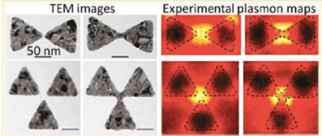
Metallic nanostructures have the unique ability to concentrate light on the nanoscale, thus they en- able a powerful marriage between photonics and nanotechnology. This concentration of electromag- netic energy is similar to that of well-known cell phone antennas, but occurs at optical frequencies. When light falls on a metal nanostructure, it can set the conduction electrons within the metal in motion, and for specific frequencies electro- magnetic resonances can arise. These so called localised surface plasmon resonances depend on the shape, size, and the immediate dielectric sur- rounding of the nanostructure. On resonance, light is tightly confined to the surface of the nanostruc- ture, until it gets eventually absorbed inside the metal, or scattered back into photons. This effect is all around us - in its most spectacular form in stained glass.
Using modern nanofabrication methods such as electron beam lithography or focused ion beam milling, we can now create metallic nanostructures with very defined plasmon resonances. This lays the groundwork for a whole set of promising applications, be it in biosensing, the development of nanolasers, or structures for enhancing the emission of quantum dots or the efficiency of solar cells.
Recognition
In 2010 the pioneering nanoplasmonics work headed by Prof Stefan Maier was awarded with two distinguished prizes – the international Sackler Prize in the Physics Sciences, awarded by Tel Aviv University, and the Paterson Medal of the Institute of Physics.
Biological sensing
PLASMONICS FOR BIOLOGICAL SENSING
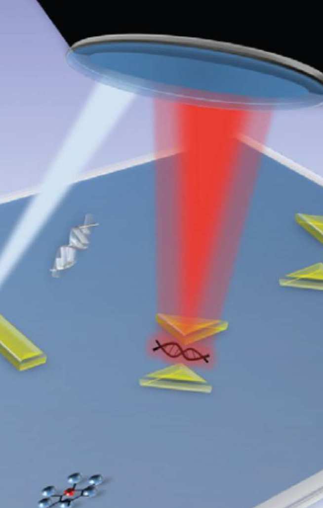
The field of plasmonics uses collective electronic resonances in metal nanostructures to compress light fields into tiny volumes, often much less than an optical wavelength. Such structures can be designed to concentrate light to enable extremely sensitive chemical detection, down to just a handful of biomolecules, via a dramatic amplifica- tion of their optical absorption characteristics. Similar approaches are being pursued at the other end of the spectrum, where we use designer “spoof plasmon” surfaces to confine THz radiation close to the surface where it can be strongly absorbed. A well-known example of devices relying on localised plasmon resonances are glucose-sensors for diabetics.
SERS, surface enhanced Raman Spectroscopy, exploits the same plasmonic field enhancement effect to achieve enhancement of vibrational coupling of molecules to light by many orders of magnitude. Imperial researchers led by Prof Cohen developed the use of coupled plasmons between colloidal gold nanostructures to move towards a method capable of detecting disease-specific enzymes with unprecedented levels of sensitivity.
Nanolasers
Plasmonic lasers focus optical energy in both time and space to generate extremely intense light at the nanoscale. Dr Rupert Oulton, an EPSRC Career Advancement Fellow and Leverhulme Lecturer in Plasmonics and Metamaterials, is currently developing such laser devices. Light at length scales of just ten billionths of a metre and lasting for just one trillionth of a second drastically alters the strength of light-matter interactions to vastly improve the sensitivity of conventional spectroscopies and the data capacity of optical communications.