Research areas in optoelectronic materials development
- Atmospheric pressure - chemical vapour deposition (AP-CVD)
- Vapour-based deposition methods
- Growth from solution
- Spectroscopic characterisation
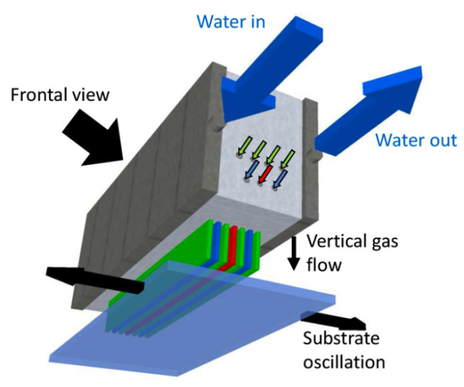
Atmospheric pressure chemical vapour deposition (AP-CVD) is a vapour-based technique we use to grow functional oxide thin films. The reactor is comprised of a gas manifold (Fig. 1), in which the vapour-based metal precursor, oxidant and inert gases are introduced via separate channels. From these header channels, the precursor gases are vertically introduced to the substrate. The substrate is oscillated underneath these gas channels, such that the precursors chemisorb and react to form oxide layers. By repeatedly oscillating the substrate underneath the gas manifold, the oxide thickness can be controlled. We have grown a wide range of n- and p-type oxides and we find that the films have a similar uniformity and density as atomic layer deposited oxide films. Additionally, the AP-CVD films are conformal to high aspect ratio nanostructures. Importantly, we are able to grow these films two orders of magnitude faster than atomic layer deposition without the need for a vacuum chamber. This makes the process appealing for growing oxides at scale, as well as growing oxides over thermally-sensitive semiconductors. We have applied the oxides grown (e.g., ZnO, NiO) as charge transport layers in solar cells, charge injector layers in light-emitting diodes, as well as the active layer in thin film transistors. Through AP-CVD, we can tune the properties of our films over a wide range through the growth temperature, oxidant used and alloying our oxides with other elements.
Further reading
Details on our AP-CVD reactor: Robert L. Z. Hoye, et al. Synthesis and modeling of uniform complex metal oxides by close-proximity atmospheric pressure chemical vapor deposition. ACS Applied Materials & Interfaces, 2015, 7(20), 10684-10694.
Growth of multi-component oxides: Robert L. Z. Hoye, et al. Improved Open‐Circuit Voltage in ZnO–PbSe Quantum Dot Solar Cells by Understanding and Reducing Losses Arising from the ZnO Conduction Band Tail. Advanced Energy Materials, 2014, 4(8), 1301544.
Rapid deposition of buffer layers on perovskite solar cells: Ravi D. Raninga,† Robert A. Jagt,† ..., Robert L. Z. Hoye. Strong performance enhancement in lead-halide perovskite solar cells through rapid, atmospheric deposition of n-type buffer layer oxides. Nano Energy, 2020, 75, 104946.
†Equal contribution
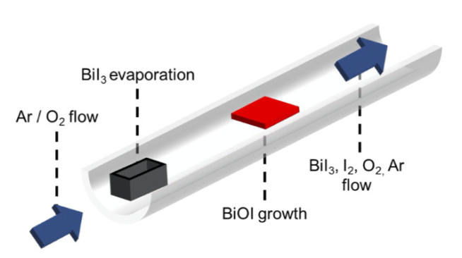
We have developed physical and chemical vapour-based methods to grow new solar absobers. These are scalable methods comprised of a horizontal tube heated with a two-zone furnace. The precursor (e.g., BiI3 for growing BiI3 by physical vapour transport or BiOI by chemical vapour deposition) is vapourised in the first zone and is carried to the second zone by an inert gas. In chemical vapour transport or chemical vapour deposition, we introduce oxygen gas to grow oxyhalides. We have used these growth systems to synthesise halide and oxyhalide thin films for investigation in photovoltaics, as well as single crystals to understand the fundamental properties of the materials.
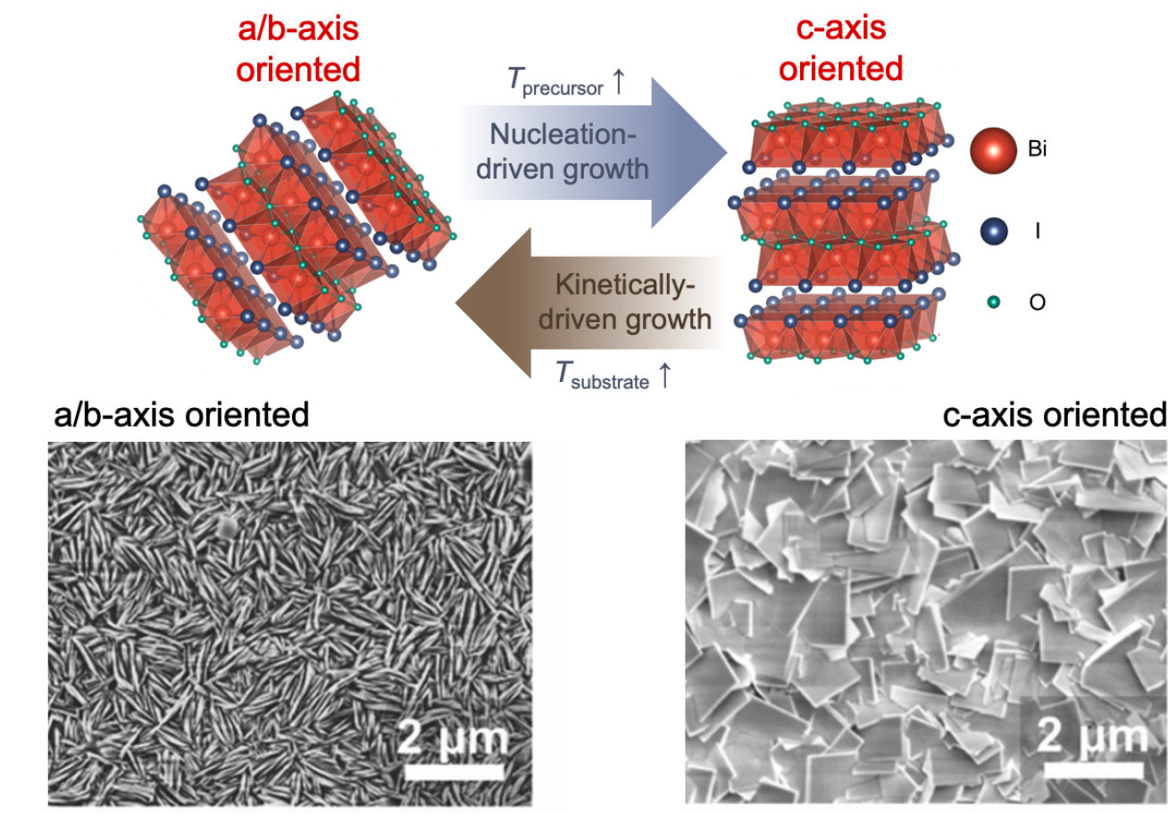
As a recent example of our work, we have systematically identified the growth mechanism of BiOI thin films by chemical vapour deposition. We showed that growth was mass-transport limited, and that the preferred orientation can be controlled through the source and substrate temperatures, which determine whether growth is nucleation- or kinetically-driven.
Read more: Robert A. Jagt, ..., Robert L. Z. Hoye. Controlling the preferred orientation of layered BiOI solar absorbers. Journal of Materials Chemistry C, 2020, Advance Article. DOI: 10.1039/D0TC02076A
*Both figures reprinted with permission from J. Mater. Chem. C, 2020, Advance Article. DOI: 10.1039/D0TC02076A. Published by the Royal Society of Chemistry
Further reading
CVD of BiOI and the effect of substrate: Robert L. Z. Hoye, et al., Strongly Enhanced Photovoltaic Performance and Defect Physics of Air‐Stable Bismuth Oxyiodide (BiOI). Advanced Materials, 2017, 29(36), 1702176.
Physical vapour transport of BiI3: Riley E. Brandt, et al., Investigation of Bismuth Triiodide (BiI3) for Photovoltaic Applications. The Journal of Physical Chemistry Letters, 2015, 6(21), 4297-4302.
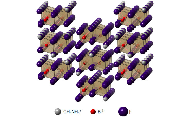
We have developed routes to synthesise exotic functional thin films by solution-based methods. One example is methylammonium bismuth iodide, which is comprised of a hexagonal unit cell with isolated bismuth-halide groups alternating with methylammonium cations (Fig. 4). We were among the first to investigate this material as solar absorbers and achieved phase-pure compounds by reacting bismuth iodide thin films, deposited by solution processing, with methylammonium iodide in solution or in the vapour phase. Films made by vapour-assisted conversion gave long photoluminescence lifetimes of 8.1 ns. Another example of a material we developed a solution-based synthesis route for was Cs2Ag(SbxBi1-x)Br6 double perovskite alloys. We achieved alloying over the entire composition range, from pure Sb- to pure Bi-based double perovskites. In doing so, we showed that this alloy system exhibited substantial band gap bowing, such that the mixed alloys exhibited a lower band gap than either pure compound. By working with theorists, we found that this was due to the Type II band alignment between Cs2AgBiBr6 and Cs2AgSbBr6, and non-linear mixing of the Bi and Sb atomic orbitals.
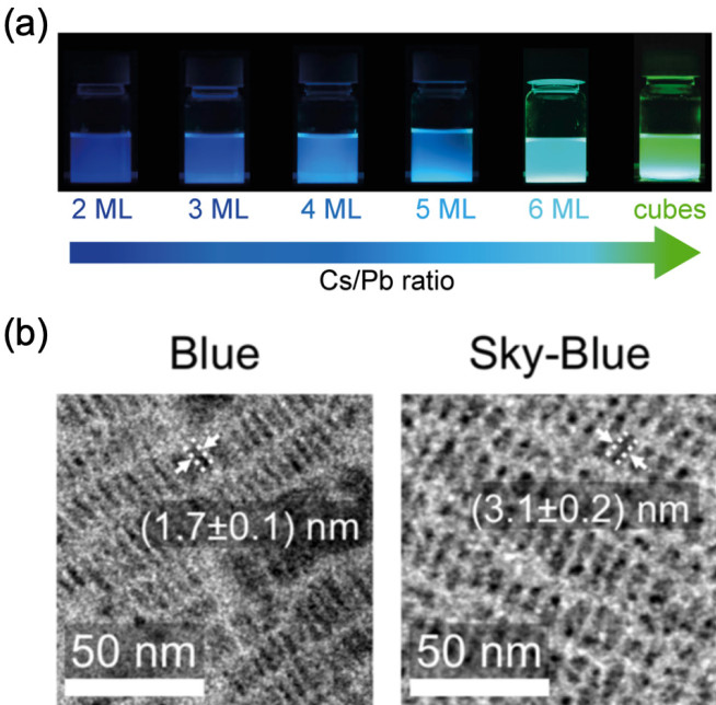
Beyond perovskite-inspired materials, we have also worked on the synthesis and application of nanostructured lead-halide perovskites for light-emission applications. Working with collaborators at Ludwig Maximilians University in Munich, we have synthesised CsPbBr3 perovskite nanoplatelets. Quantum confinement results in a blue-shift in the emission wavelength. This emission is easily tunable through the number of monolayers (Fig. 5a), which can be adjusted through the volume of precursors used in the ligand-assisted reprecipitation synthesis method. Monodisperse nanoplatelets are achievable (Fig. 5b). By passivating the surface defects on the nanoplatelets with PbBr2 complexed with organic ligands, we can achieve high photoluminescence quantum efficiencies >60%. With these nanoplatelets, we have achieved sharp, colour-pure electroluminescence in the blue (460 nm) and sky-blue (490 nm) wavelength ranges. These can be used as saturated blue emitters for ultrahigh definition displays, or in flexible white light emitting diodes.
In addition, we are working with Dr. Laura Torrente and Dr. Sam Stranks (Chemical Engineering, University of Cambridge) on growing perovskite nanocrystals using a flow reactor. This could allow small nanocrystals to be achieved (resulting in blue emission through quantum confinement), or allow core-shell structures to be synthesised.
Further reading
Double perovskites: Zewei Li,† Seán R. Kavanagh,† et al., Bandgap lowering in mixed alloys of Cs2Ag(SbxBi1-x)Br6 double perovskite thin films. J. Mater. Chem. A, 2020, 8, 21780-21788.
†Equal contribution
Perovskite nanoplatelet synthesis and properties: Bernhard J. Bohn,† Yu Tong,† et al., Boosting tunable blue luminescence of halide perovskite nanoplatelets through post-synthetic surface trap repair. Nano Letters, 2018, 18(8), 5231-5238.
†Equal contribution
Perovskite nanoplatelet LEDs: Robert L. Z. Hoye,† May-Ling Lai,† et al., Identifying and Reducing Interfacial Losses to Enhance Color-pure Electroluminescence in Blue-emitting Perovskite Nanoplatelet Light-emitting Diodes. ACS Energy Letters, 2019, 4, 1181-1188.
†Equal contribution
Review on defects in perovskites: Junzhi Ye, et al., Defect Passivation in Lead-Halide Perovskite Nanocrystals and Thin Films: Toward Efficient LEDs and Solar cells. Angewandte Chemie - International Edition, 2021, 60, 2-27; Angewandte Chemie, 2021, 133, 2-27
Review on perovskite nanocrystals: Amrita Dey, Junzhi Ye, ... Robert L. Z. Hoye,* Lakshminarayana Polavarapu.* State of the Art and Prospects of Halide Perovksite Nanocrystals. ACS Nano, 2021, Article ASAP. DOI: 10.1021/acsnano.0c08903
Invited review selected ACS Editor's Choice
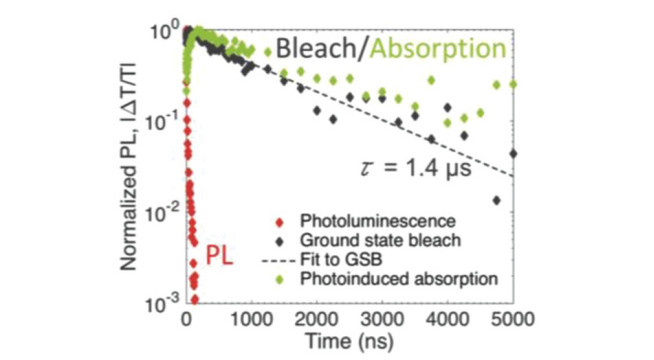
The key properties of new solar absorbers that determine their suitability for photovoltaics are: 1) the band gap and absorption coefficient, 2) minority-carrier lifetime, 3) photoluminescence quantum yield and 4) electronic structure. We have access to a suite of facilities to evaluate these properties. These include time-correlated single photon counting to measure the photoluminescence lifetime, as well as photoluminescence mapping techniques with a confocal microscope. We also collaborate with the Optoelectronics Group (Cavendish Laboratory, Cambridge) to understand the photophysics of our materials by transient absorption spectroscopy. The kinetics of charge carriers are influenced by disorder and traps within the bandgap. To measure these parameters, we use photothermal deflection spectroscopy, with which we can measure the sub-bandgap absorbance. We correlate the kinetics and defect structure of the material to the electronic structure using photoemission spectroscopy, which provides information on the composition, bonding states of the surface elements, as well as valence band states.
Further reading
Spectroscopy on Cs2AgBiBr6: Robert L. Z. Hoye, et al., Fundamental Carrier Lifetime Exceeding 1 µs in Cs2AgBiBr6 Double Perovskite. Advanced Materials Interfaces, 2018, 5(15), 1800464.
Characterisation of the defect tolerance of BiOI: Tahmida N. Huq,† Lana C. Lee,† ..., Robert L. Z. Hoye. Electronic Structure and Optoelectronic Properties of Bismuth Oxyiodide Robust against Percent‐Level Iodine‐, Oxygen‐, and Bismuth‐Related Surface Defects. Advanced Functional Materials, 2020, 30(13), 1909983.
†Equal contribution
Best practices in characterisation: Robert L. Z. Hoye, et al., Perovskite-inspired photovoltaic materials: Toward best practices in materials characterization and calculations. Chem. Mater., 2017, 29, 1964.