Research into advanced energy devices
- Next-generation solar photovoltaics
- Indoor photovoltaics
- Tandem solar cells
- Light-emitting diodes
- Photoelectrochemical cells
We work on developing thin film solar cells based on emerging materials. In the past few years, we have worked with colloidal quantum dot absorbers, polymers, cuprous oxide, as well as ns2 compounds predicted to be defect-tolerant. We have developed a wide range of charge transport layers for optimal carrier extraction and to control non-radiative losses at the interfaces. Our work heavily focusses on understanding the processes limiting device performance, such as through optical loss analyses, transient photovoltage measurements, intensity-dependent device measurements and white-light biased external quantum efficiency measurements. In numerous cases, we have devised strategies to achieve improved performance over the state-of-the-art.
Further reading
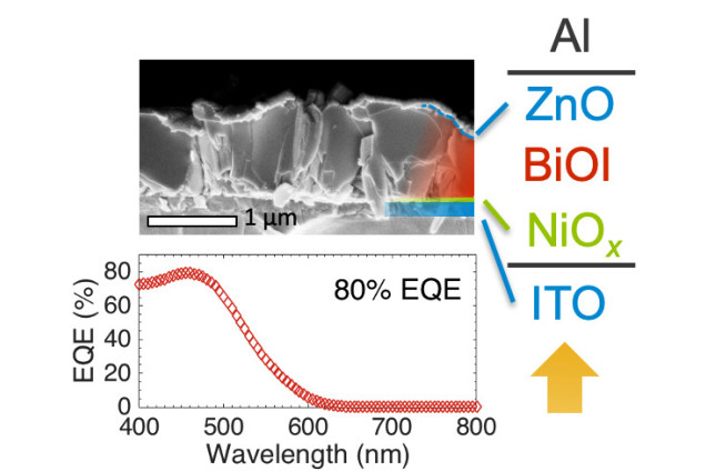
BiOI solar cells: Robert L. Z. Hoye, et al., Strongly Enhanced Photovoltaic Performance and Defect Physics of Air‐Stable Bismuth Oxyiodide (BiOI). Advanced Materials, 2017, 29(36), 1702176. Press release
Perovskite solar cells with oxide buffer layers: Ravi D. Raninga,† Robert A. Jagt,† ..., Robert L. Z. Hoye. Strong performance enhancement in lead-halide perovskite solar cells through rapid, atmospheric deposition of n-type buffer layer oxides. Nano Energy, 2020, 75, 104946.
†Equal contribution
Colloidal quantum dot solar cells: Robert L. Z. Hoye, et al., Improved Open‐Circuit Voltage in ZnO–PbSe Quantum Dot Solar Cells by Understanding and Reducing Losses Arising from the ZnO Conduction Band Tail. Advanced Energy Materials, 2014, 4(8), 1301544.
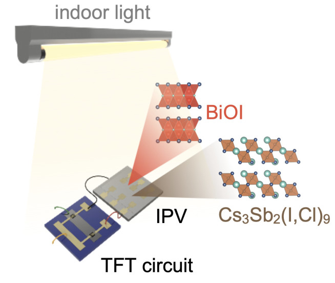
The Internet of Things (IoT) describes an ecosystem of interconnected devices, creating smart homes and workplaces. It is predicted by by 2025, there will be 75 billion devices part of the IoT ecosystem. Many of these devices will be small, autonomous and located in remote locations. Powering all of these devices with batteries will no longer be practical or sustainable, given the presence of scarce and, in some cases, toxic elements in batteries. Using photovoltaics to harvest indoor light is a promising alternative.
We demonstrated that lead-free perovskite-inspired materials (PIMs) are promising as indoor photovoltaics (IPV). Recently, we tested two PIMs (BiOI and Cs3Sb2(I,Cl)9) for IPV, and demonstrated efficiencies within the range of commercial technologies. We calculated the optically-limited efficiencies of these materials and other PIMs, showing that fully optimised devices could reach efficiencies of 40-60%, far surpassing devices based on hydrogen-passived amorphous silicon, which is the current industry standard for IPV.
Further reading
Yueheng Peng,† Tahmida N. Huq,† Jianjun Mei,† ..., Robert L. Z. Hoye,* Vincenzo Pecunia.* Lead-Free Perovskite-Inspired Absorbers for Indoor Photovoltaics. Advanced Energy Materials, 2021, 11, 2002761.
†Equal contribution
Vincenzo Pecunia,* Luigi G. Occhipinti, Robert L. Z. Hoye.* Emerging Indoor Photovoltaic Technologies for Sustainable Internet of Things. Advanced Energy Materials, 2021, 2100698. Early View, DOI: 10.1002/aenm.202100698
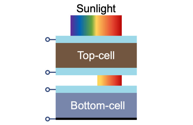
Tandem photovoltaics combine multiple solar cells (Fig. 3) to increase the fraction of the solar spectrum converted to electrical energy, allowing single-junction device efficiency limits to be overcome. We have developed tandems between metal-halide perovskite top-cells (visible light absorbers) and silicon bottom cells (near-infrared light absorbers) in a monolithic configuration, achieving high performance and stable device operation. Our focus in this area is in: 1) developing recombination contacts that couple together both sub-cells to achieve voltage addition with minimal parasitic optical losses, 2) developing tandems using industrially-relevant bottom cells, and 3) faster methods to grow the oxide buffer layer protecting the perovskite top cell. For example, in 2016, we developed an ITO/NiOx recombination contact. In collaboration with Stanford, Arizona State University and others, this led to a 23.6%-efficient two-terminal tandem, which became the first entry for perovskite-silicon tandems on the NREL chart of best research-cell efficiencies.
Further reading
Collaborative work with Stanford, ASU and others: Kevin A. Bush,† Axel F. Palmstrom,† J. Yu Zhengshan,† et al., 23.6%-efficient monolithic perovskite/silicon tandem solar cells with improved stability. Nature Energy, 2017, 2(4), 17009.
†Equal contribution
First monolithic perovskite tandem with industrially-common p-type silicon: Robert L. Z. Hoye,† Kevin A. Bush,† et al., Developing a robust recombination contact to realize monolithic perovskite tandems with industrially common p-type silicon solar cells. IEEE Journal of Photovoltaics, 2018, 8(4), 1023-1028.
†Equal contribution
Oxide buffer layers: Robert A. Jagt, ..., Robert L. Z. Hoye. Rapid Vapor-Phase Deposition of High-Mobility p-Type Buffer Layers on Perovskite Photovoltaics for Efficient Semitransparent Devices. ACS Energy Letters, 2020, 5, 2456-2465. Press release
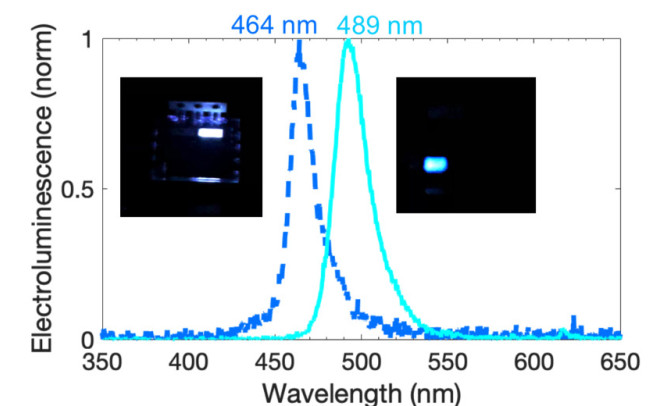
Light-emitting diodes are the inverse of photovoltaics: Electrons and holes are injected to an active layer to achieve electroluminescence. Over the past few years, we have worked primarily on metal-halide perovskite emitters. We have developed device structures that reduce non-radiative losses and more effectively confine electrons and holes within the emissive layer to give colour-pure electroluminescence. A particular advantage of metal-halide perovskites is that their low levels of disorder result in sharper electroluminescence peaks than conventional inorganic and organic materials, making the perovskites particularly appealing for ultrahigh definition display applications.
Further reading
Review on factors influencing light-emission in perovskites: Samuel D. Stranks, Robert L. Z. Hoye, et al., The physics of light emission in halide perovskite devices. Advanced Materials, 2019, 31(47), 1803336.
Sharp emission in green LEDs: Robert L. Z. Hoye, et al., Enhanced performance in fluorene‐free organometal halide perovskite light‐emitting diodes using tunable, low electron affinity oxide electron injectors. Advanced Materials, 2015, 27(8), 1414-1419.
Blue perovskite nanoplatelet LEDs: Robert L. Z. Hoye,† May-Ling Lai,† et al., Identifying and reducing interfacial losses to enhance color-pure electroluminescence in blue-emitting perovskite nanoplatelet light-emitting diodes. ACS Energy Letters, 2019, 4(5), 1181-1188.
†Equal contribution
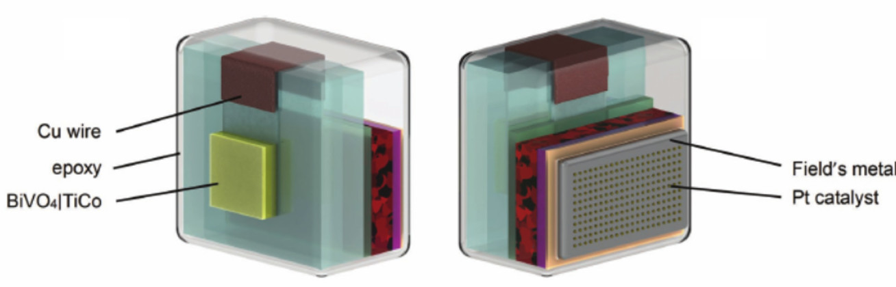
Our primary focus is on optoelectronic materials for photovoltaics and LEDs. But there is strong overlap in the properties of solar absorbers, light-emitting and photocatalysts. The materials we have been developing (e.g., lead-halide perovskites, but also the lead-free materials) have suitable band positions for water reduction and, in some cases, oxidation as well. We work in collaboration with the Reisner Group (Chemistry, University of Cambridge) in the development of these materials for photoelectrochemical cells.
Further reading
Perovskite photocathodes for water splitting: Virgil Andrei, Robert L. Z. Hoye, et al., Scalable Triple Cation Mixed Halide Perovskite–BiVO4 Tandems for Bias‐Free Water Splitting. Advanced Energy Materials, 2018, 8(25), 1801403.