 The current trend in MOSFET downscaling, for increased speed and packing density, has led to 3D device structures such as finFETs and (GAA) gate-all-around FETs or simply, nanowire-based FETs with multiple gates for increased control. Further developments in this field are driven by technology computer aided design (TCAD) in which e.g. geometry optimisation can be investigated for increased performance or increased functionality. In our group, this has led to novel devices and structures such as the SGrFET (Screen Grid FET), the Y-branch FET and the Unipolar Nanowire Rectifier that can also be used for nano-contact optimisation.
In addition to FET development via TCAD, our group is also involved in low frequency noise characterisation of devices, including different types of FETs and spintronics devices. Low frequency noise is a powerful tool to investigate the influence of material imperfections on device characteristics. It is therefore also a tool that can be exploited for the sensing of molecule on the surface of FET-alike devices.
articles
- TCAD
- Noise in semiconductor devices
- Strained-Si Field Effect Transistors
- Substrates for Strained-Si-on-Insulator
- Si:SiGe Mosfet-on-Air Through Post-Processing Techniques
- Low Temperature and Noise Modelling in Strained-Si FETs
- CABOOM: Characterisation of Alloy concentration by Bevelling, Oxidation and Optical Microscopy
- BKFM: Kelvin Probe Microscopy on bevelled samples as material characterisation technique
- Combined Raman - Atomic Force Microscope
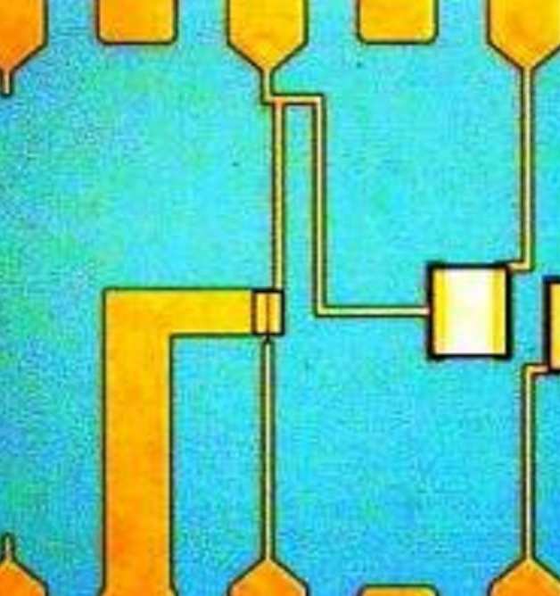
The screen-grid FET is a field effect transistor where the gating action is perpendicular to the current flow via cylindrical gates inside the channel of a thin body SOI structure. TCAD modelling promises increased digital functionality and robustness under aggressive downscaling. The particular geometry of the SGrFET allows its use as a coulter counter sensor that is able to actively sense and amplify the signal of passing bio-particles.
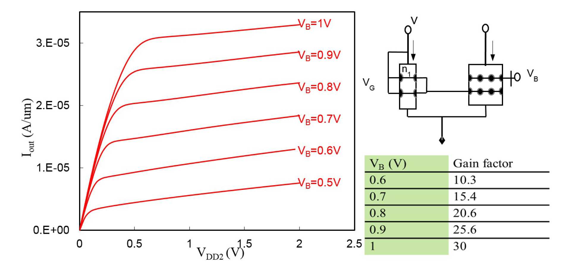
Tuneable Current Mirror as a function VB [Fobelets K, Ding P.W., Shadrokh Y. and Velazquez-Perez J.E., “Analog and digital performance of the Screen-Grid Field Effect Transistor (SGrFET)”, International Journal of High Speed Electronics and Systems (IJHSES) 18(4), Chapter 1 (2008) – best invited paper award]
The Unipolar Nanowire Rectifier is a nanowire device of one doping type in which, at one side of the nanowire the ohmic contact to the cross section of the wire overlaps over a certain distance with the oxide coated cylindrical nanowire surface. This can deplete the nanowire whilst maintaining an ohmic contact and thus creates a rectifying behaviour. In the other bias condition it will increase the free carrier concentration and improve the ohmic contact to the nanowire. This method can be applied to improve ohmic contacts to nanowire devices.
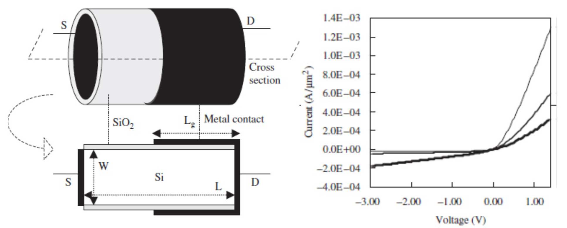
Current-voltage characteristics of a 50 nm diameter unipolar nanowire with a metal side gate overlap of L= = 50, 100 and 150 nm. The highest current in “forward” bias is associated to the largest overlap. [K. Fobelets, and J.E. Velazquez-Perez, “Rectification in unipolar nanowires”, Physica E: Low-Dimensional Systems and Nanostructures, 40(7), 2481-2484 (2008)]
Low frequency noise is a tool to analyse some basic parameters in semiconductor devices. We have applied this tool extensively to the study of globally-strained modulation doped field effect transistors in Si/SiGe technology. One of our main results is that the original of the noise in n and p strained buried channel devices is the same as that for the n and p channel MOSFETs and can, in all cases, be explained by the McWorther model of carrier fluctuations.
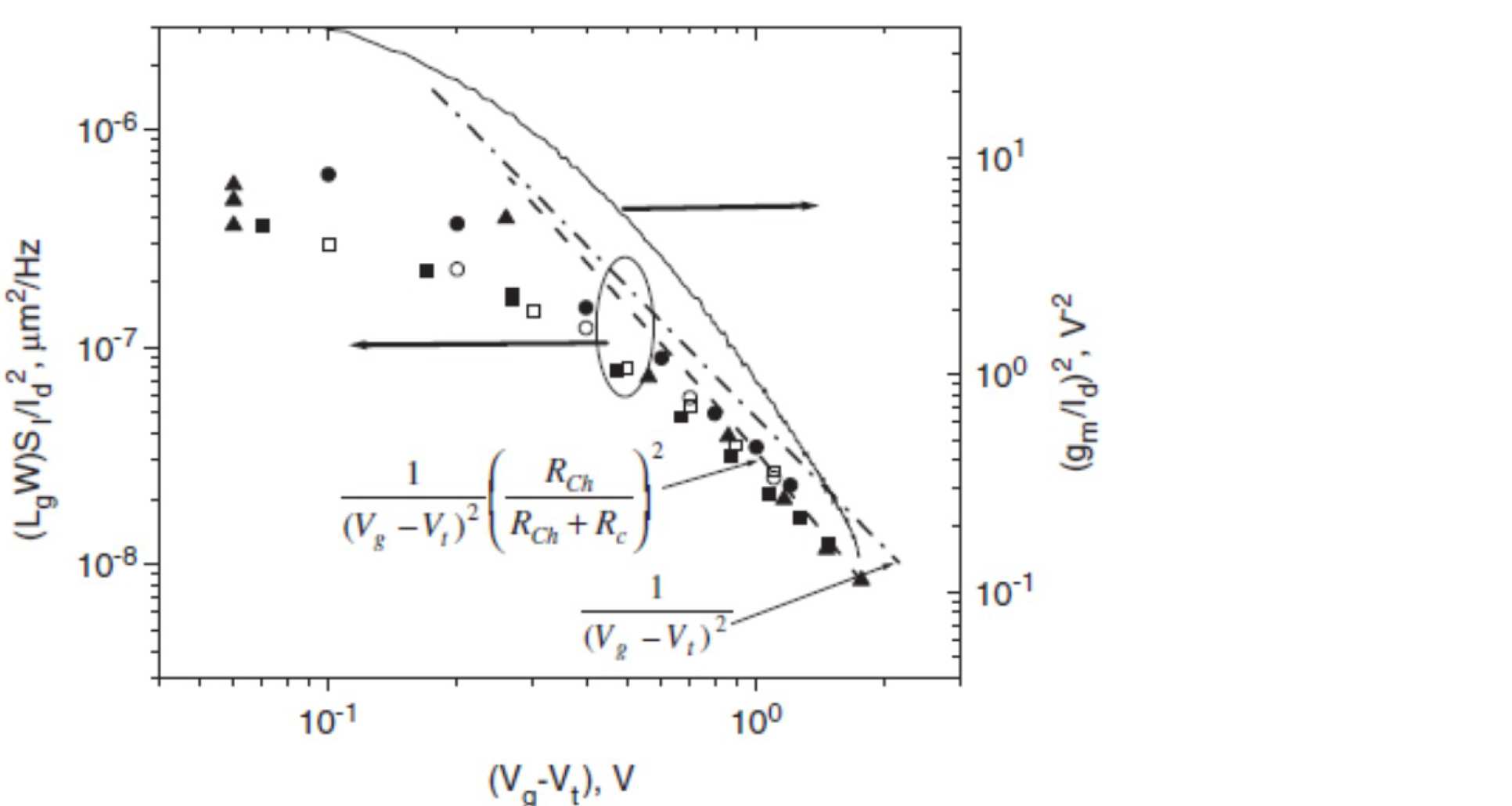
Relative spectral noise density (left) as a function of gate voltage overdrive for strained-Si MOSMODFETs (filled symbols) and Si MOSFETs (open symbols). The dashed and dashed/dotted lines show the slopes in accordance with the McWorther model with and without correction on the contact resistance. [S. L. Rumyantsev, K. Fobelets, T. Hackbarth, M. S. Shur, “Low frequency noise in insulated-gate strained-Si n-channel modulation doped field effect transistors”, Jap. J. Appl. Phys. 46(7A), pp. 4011-4015 (2007).]
Low frequency noise can also be used for increasing the selectivity of molecule sensing, e.g. NH3 and NO2 sensing in a humid environment. Since low-frequency noise is very sensitive to surface states, interaction that happen at the surface between these states and the adsorbing molecules will lead to changes in the noise character of the devices. We have applied this technique to NH3 and NO2 sensing in a humid environment using n and p-type Si nanowire arrays and measuring both conductivity changes and noise changes. This allows us to distinguish between the two gases without functionalisation of the wires. Noise changes in those cases where the adsorbing gases inject minority carriers into the nanowires.
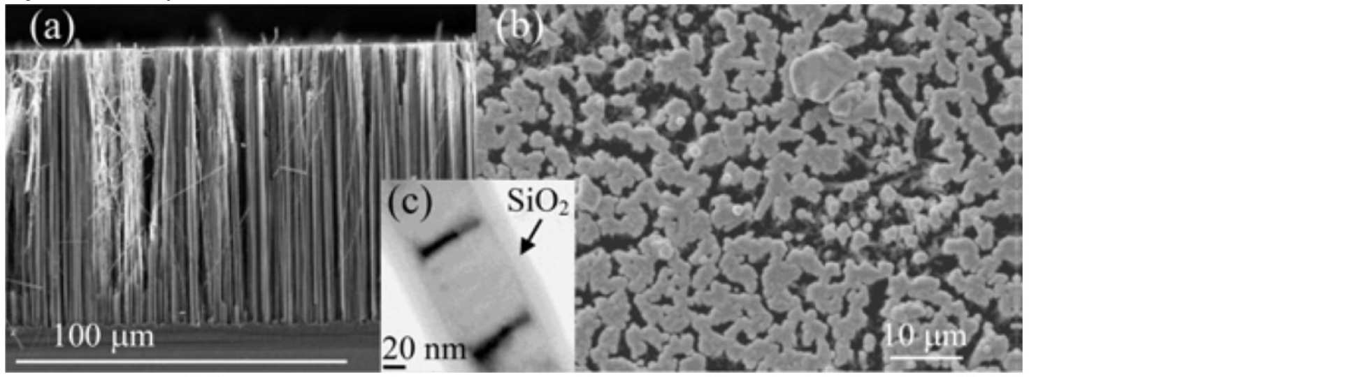
SEM pictures of the nanowires array, cross section view and top view after metallisation. Inset: TEM of one nanowire.
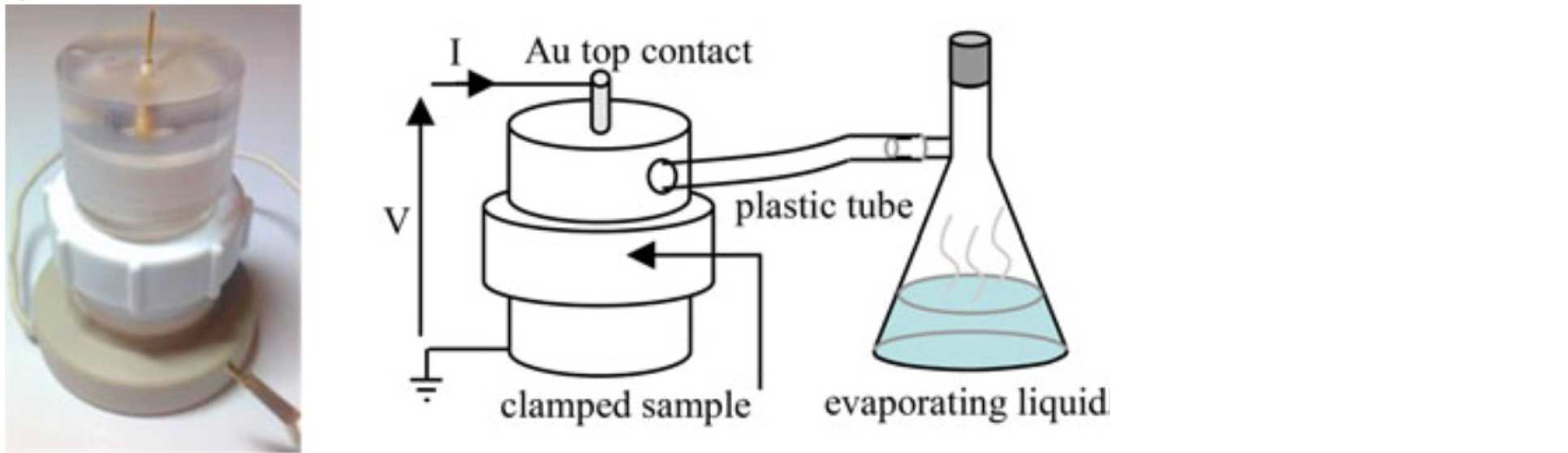
Experimental setup to contact the nanowires within an enclosed environment into which the gasses are diffusing.
[K. Fobelets, Meghani M.; Li C., “Influence of Minority Carrier Gas Donors on Low Frequency Noise in Silicon Nanowires”, IEEE Trans. Nanotechnol. 13(6), 1176-1180 (2014) ]
Kristel Fobelets, Christos Papavasilliou
Research into the performance improvements offered by strained-Si technology in micro-power circuits was funded by EPSRC within the national UK research effort on strained-Si HMOS for future CMOS. Both strained-Si buried channel and surface channel FETs were investigated for their sub-threshold performance at DC, RF and over a temperature range between 10K and 350K. The key result of this investigation is that strained-Si technology offers ultimate potential for low power RF applications while circumventing aggressive scaling with its associated increase in power consumption and cost.
 |
|---|
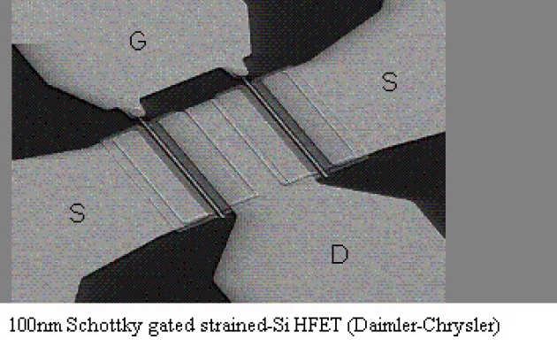
In this research we have demonstrated the superiority of the Schottky gated buried channel Si:SiGe HFETs for low power operation via RF characterisation and comparison to state-of-the-art Si nMOS. We designed and characterised simple monolithically integrated strained-Si circuits, both buried channel and surface channel, operating in sub-threshold and showing remarkable linearity and cut-off frequencies within the low gate and drain voltage range applied.
Examples are a single stage amplifier driven below threshold (VDS<0.3V, VGS<-0.2V) with 15 dB gain @ 26 µW input power and a bandwidth of 38 MHz ; and a monolithically integrated current mirror with a linearity over 4 decades at room temperature reducing to 1 decade at 160K whilst consuming only 100 ?W at room temperature reducing to 10-3 ?W at 160K. Interesting results on device research is that we have demonstrated via low temperature measurements and comparison to nMOS processed in the same run, that for both MOS-gated strained-Si buried channel and surface channel devices the performance improvement is due to improved phonon scattering characteristics of the strained-Si FETs down to a temperature of 100K. Below 100K the enhanced performance of strained-Si devices is solely a result of the improved effective mass in the strained-Si channel. Whilst RF performance improvement of Schottky-gated buried channel FETs had already been proven, we are the first to demonstrate RF performance improvements of MOS-gated buried channel FETs as a results of careful layer design, growth and processing parameters.
 |
|---|
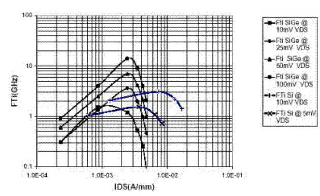
| Intrinsic cut-off frequency vs. current density of a 100nm gate length HFET (100?m gate width) and Si MOSFET (blue lines) (40?m gate width) for different VDS values. |
Kristel Fobelets
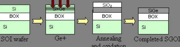
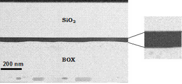
On the one hand SOI (Silicon-on-Insulator) has been accepted in mainstream CMOS technology and on the other hand strained-Si is being considered as an alternative MOS material, therefore the need for strained-Si-on-insulator is appearing. Different fabrication techniques exist, based on adapted SIMOX and Bonded-etch-back techniques. We (H.S. Yuk and T. Tate) have developed a novel technique GISOI – Ge+ implantation into commercial SOI to fabricate SGOI. By controlling the implantation and anneal ambient, we have been able to fabricate a 50nm thick SiGe layer on insulator with a Ge concentration of 34%, a relaxation degree of 98%, an estimated dislocation density below 10-5 cm-2 and a surface roughness of 0.44 nm RMS. This SGOI layer can then be used to grow a strained-Si channel for PDSOI technology, or this substrate can be used to further increase the Ge concentration via the Ge condensation technique for GOI. Ge condensation is the technique that increases the Ge concentration in a SiGe layer sandwiched between two SiO2 layers. The available Ge gets trapped between the SiO2 while Si is consumed in the oxidation process. Oxidation time, temperature and thickness of the starting material are all critical parameters in this process. We are currently investigating the difference between the Ge condensation process in GISOI wafers and SOI wafers with an extra MBE grown SiGe top layer. The main difference between the two is the degree of crystalinity of the starting material. We (B. Vincent) have found that at high temperatures and low SiGe layer thicknesses, the Ge atoms disappear rapidly from the SiO2 sandwich, presumably as a consequence of the lack of further Si atoms for the oxidation process.
 |
|---|
 |
|---|
| An XTEM image (Univ. of Sheffield) of and GISOI sample implanted at 550ºC, annealed at 1200 ºC for 180 minutes under pure oxygen |
Kristel Fobelets, S.M. Li
Completely processed MOS-gated Si/SiGe n-channel Modulation Doped Field Effect Transistors (MODFETs) have been post-processed to remove the Si substrate and part of the SiGe virtual substrate to construct strained-Si MOSFETs-on-air. The resulting substrate thickness underneath the devices was reduced down to 2 ?m after thinning and a flip-chip process was developed to transfer the devices to an insulating carrier substrate. A post-processing technology was developed for heat sensitive devices. The membrane devices, surrounded by air, were characterised after thinning and compared to the un-thinned characteristics. A large reduction of the off-currents of the MODFETs on air, due to an increase in substrate resistance, has been measured, making them more suitable for low power applications. Further relaxation of the substrate during substrate thinning causes a shift in the threshold voltage.
 |
|---|
| Thinned devices front and back |
Jesus-Enrique Velazquez-Perez (Univ. Salamanca), Kristel Fobelets
Commercial TCAD available today for physical simulation of semiconductor devices, lacks suitable models for the carrier mobility in the layers of modern transistors. This is due to a) the complexity of the transport in sub-micron devices and b) most of the TCAD development has been driven by bulk CMOS, thus accurate general closed-form mobility expressions are lacking for e.g strained-Si FETs and low temperature operation. Nevertheless, present TCAD device simulators (such as Taurus-MediciTM from Synopsys or BlazeTM by Silvaco) preserve their main strengths as a modelling tool. Our aim is thus to replace the mobility models within the commercial TCAD programs with Monte Carlo based models.
 |
|---|
Work that has been carried out is using the 2-D device simulator – MEDICI – in combination with Monte Carlo, to study different effects occurring at low temperatures in strained-Si surface and buried channel MOSFETs. We have used MEDICI to study and solve the backgating effect in these structures, to determine the origin of performance improvements, and optimize ultra thin layer MOS-MOSFETs. In the range of the expected operation frequencies (RF, microwaves and beyond) of the strained-Si circuits, the noise performance is of paramount importance as its magnitude steadily increases with the operation frequency in the above ranges. We have calculated, using MEDICI, thermal noise generated in the channel of a Si/SiGe n-MOSFET.
 |
|---|
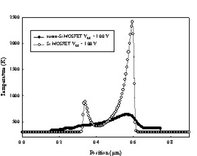
| Electron temperature’s profile in the channel of a strained-Si MOSFET and a conventional MOSFET calculated with MEDICI. |
Kristel Fobelets, Ryan Ferguson, et al.
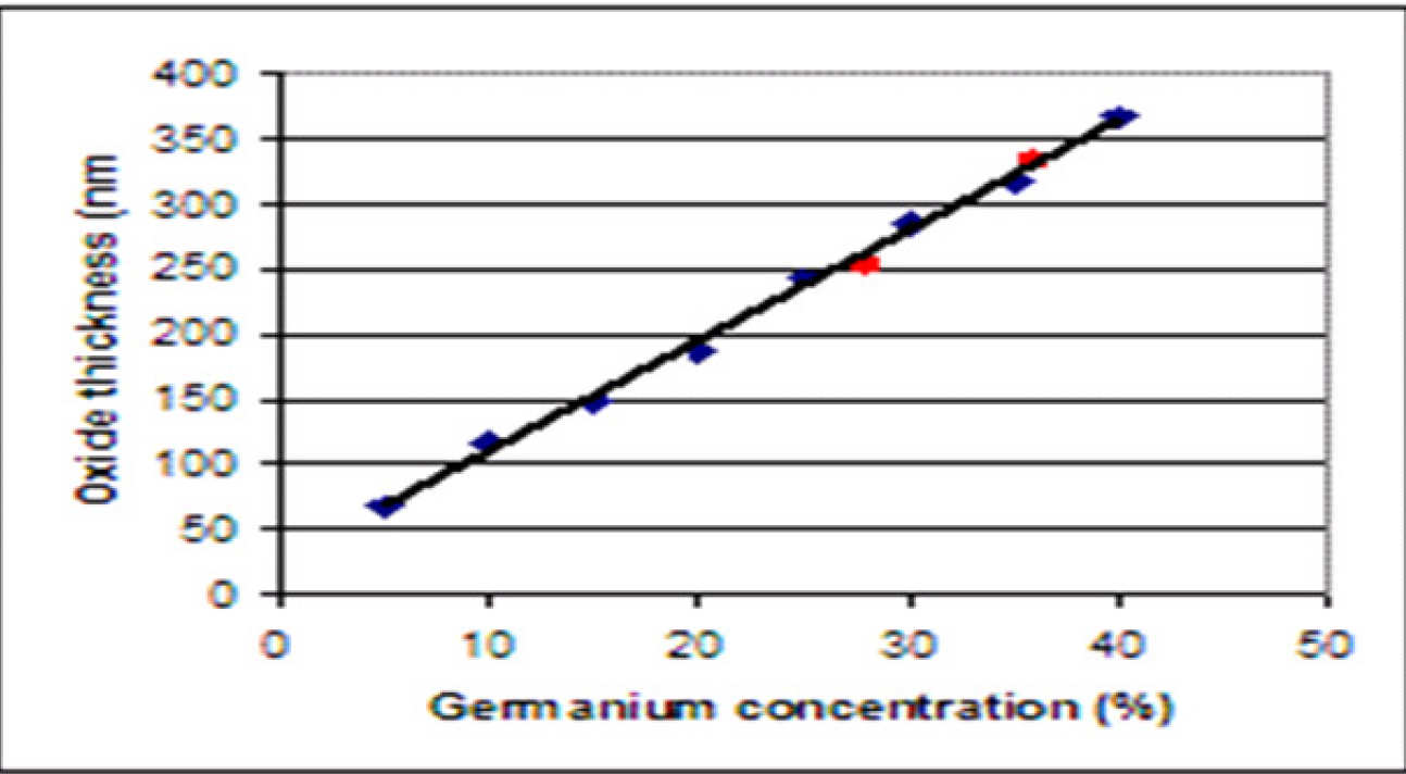
The group has invented a novel, fast and inexpensive technique to characterise the Ge concentration in heterojunctions using: a) shallow angle bevelling to present the different layers in the heterojunction at the surface, b) wet thermal oxidation will cover each layer of the heterojunction with an oxide. As the oxidation rate of SiGe is dependent on the Ge concentration the oxide thickness on the surface will be directly related to the Ge concentration in the layer underneath. c) Optical microscopy to visualise the different oxide thicknesses via diffraction. A program has been written in MathematicaTM to calculate the Ge concentration from the coloured perceived under the microscope. This program takes into account the spectrum of the microscope lamp and the sensitivity of the eye and the RGB representation on the computer screen. Currently final year project students are working to make the measurement technique of the spectrum user independent and link the measurement unit to the extraction software for automatic parameter extraction.
Fig: A heterojunction with 8 layers with different Ge concentration bevelled and oxidised, as seen under the optical microscope. The steps in Ge contents are only 5% going from 0% (left) to 40% (right). Left bottom: the output of the mathematica program gives the closest colour match and the associated Ge concentration. Below: squares are the derived oxide thickness as a function of Ge concentration for wet thermal oxidation at 700ºC for 1hr and the red circle are values found in literature for the same oxidation conditions.
 |
|---|
Leslie Cohen (Physics), Kristel Fobelets
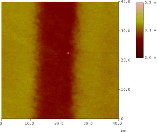
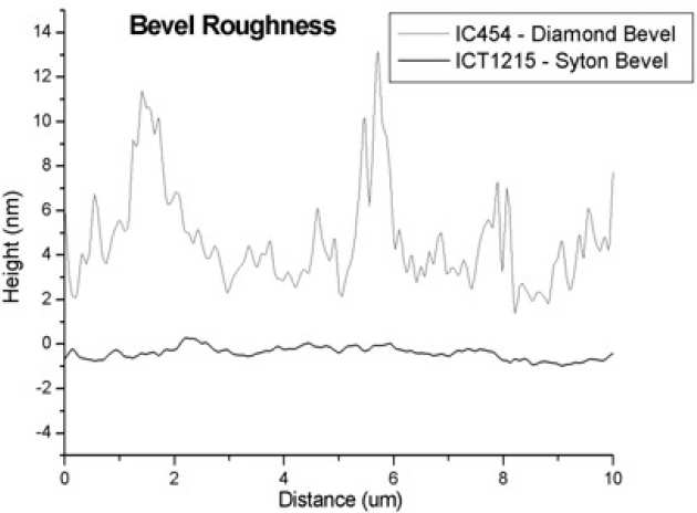
Bevelling is used in some material characterisation techniques to enlarge the width of the thin layers in heterojunctions. We have developed two new techniques to determine the thickness of the layers and the material composition based on bevelling in conjunction with Kelvin Probe Microscopy or optical microscopy after wet thermal oxidation. A chemical-mechanical polishing technique has been developed to generate nanometer smooth bevels, important to generate un-convoluted signals. Germanium quantum wells of only 7.5 nm wide have been successfully imaged using KFM, while material composition differences of only 5% can be visualised under an optical microscope. Work function differences between the different layers can be measured, and material compositions can be theoretically determined to an accuracy of 1%. This simple and in-expensive, high resolution technique might become a powerful tool in fast in-expensive material characterisation technology.
 |
|---|
| A KFM image of a 20nm InAs quantum well surrounded by GaSb cladding layers after bevelling |
 |
|---|
| Comparison between the "classical" diamond bevel and the newly developed CMP bevel roughness. |
Tom Pike, Liz Fielder, Mark Anderson (JPL)
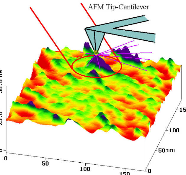
The aim of this project is to combine two existing measurement techniques - Raman spectroscopy and atomic force microscopy - to create a powerful new tool for local chemical imaging and analysis. The project is being carried out under a contract with the Jet Propulsion Laboratory.
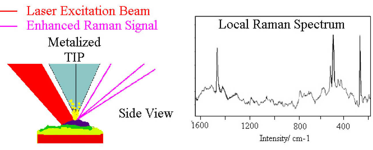
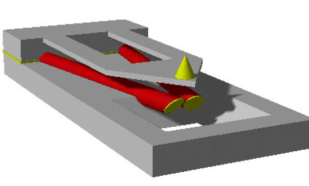
A Raman - AFM system may be constructed by metallizing the tip of an atomic force microscope, and then illuminating the tip using a laser beam. The AFM can still provide a conventional surface image, allowing features of interest to be located. However, it now also offers a means for precisely positioning a metallised nanostructure. In the vicinity of this structure, a surface enhanced Raman spectrum can be obtained, because of the increase in optical field created by the metal. This signal may be detected separately, to allow chemical analysis of the local feature. A key aim of the project will be to develop a MEMS prototype that will integrate an AFM tip with suitable illumination optics.
 |
|---|
| Principle of the Raman-AFM |
 |
|---|
| Side view of Raman-AFM, and local Raman spectrum obtained from demonstrator system |
 |
|---|
| 3D view of MEMS Raman-AFM concept. |