 Nanotechnology is the manipulation of matter, and the fabrication of structures at the scale of nanometers (10-9 meters) or even less. In practice, this covers a size scale varying from 100 nanometers to a single nanometer or even less. In particular, quantum mechanical effects become important at these scales, and become increasingly significant with the reduction in size. Nanotechnology can comprise a wide range of technological goals, from the precise manipulation of atoms and molecules in the construction of larger structures, to nanoelectronics, which focuses on the development of electronic devices with dimensions in the 1 – 100 nanometer scale, to nano-electromechanical systems (NEMS) exploiting the unique mechanical properties of nanostructures.
The Optical and Semiconductor Devices group has interests in nanotechnology within a wide range of areas, from nanostructure fabrication techniques, to the development of nanoelectronic devices less than 10 nanometers in size, to NEMS devices. Particular interests within these areas include the development of ‘beyond CMOS’ devices at the sub-10 nanometer scale for future electronic applications, practical application of quantum-effect nanoelectronic devices such as single-electron transistors and quantum dots, nanomechanical resonant structures based on suspended nanowires and nanobeams, and the development of ‘natural’ lithographic processes avoiding the need for complex nanolithographic methods.
Accordion widget
- Self-organising Resists for Nanolithography.
- Silicon Micro Contact Printing Engines
- Nanospray Dielectrophoresis
- Nanostructured Electrode Systems
- NEMS by Sidewall Transfer Lithography
- NEMS by Multilayer Sidewall Transfer Lithography
- Nanostructured 2D Cellular Materials in Silicon by STL NEMS
- Nano-Structured Silicon Implantable Lithium Batteries
- Green chemistry supercapacitors using silicon nanowires and room temperature ionic liquids
- Nanostructured Optical Materials
- Nano-scale Waveguides and Devices
- C60 nanowhiskers
- Thermoelectric Effect of One Electron
- Thermoelectric Effects in Si Nanowire Arrays
- Interactions between single charges and phonons in suspended nanocrystalline silicon nanowires
- Semiconductor device fabrication at the few nanometre scale
- Field-Effect Transistors using Chemically Etched Silicon Nanowires
- Nanowire single electron devices for ‘beyond’ CMOS application
- Novel nano-FET structure: the Screen-Grid FET
- Single-electron Transistors and Quantum Dots in Nanocrystalline Silicon
- Room temperature single nanometre scale quantum dot transistors
- Suspended Graphene on Silicon Nanowire Arrays for Enhanced Gas Sensing
- Dopant atom double quantum dots operating at room-temperature
Mino Green, Shin Tsuchiya
The conversion of thin films (thickness t) of cesium chloride into an array of hemispherical islands of narrow size distribution (average diameter D) and high packing density (3t/D) on exposure to a moist atmosphere is a useful case of "self-organization". Relatively narrow distributions (±15%D) are the general rule and a wide range of diameters (400A to 5000A) have been made. Since cesium chloride can be behave as a resist in a chlorine or fluorine plasma etch, such an array has been used for making high density pillar structures of mesoscopic dimensions. Thus pillar structures in GaAs were made (Appl. Phys. Lett. 63, 264-266 (1993)) which exhibited large size-dependent energy band shifts.
 |
|---|
| Quantum pillars in GaAs: average dia. 2500A; height 1 µm; packing density 25% |
A more comprehensive study of the process and materials parameters involved in this fabrication technique is being undertaken together with an extension of the process with a view to obtaining a narrower distribution of desired island size and higher packing density. The types of device which might benefit from a process technology dependent upon self-organizing resists and which is under consideration are: electron emitter arrays for displays etc.; high density memory arrays; substrates for the enhancement of Raman scattering; various mesoscopic semiconductor structures.
 |
|---|
| Equipment for vacuum deposition of cesium chloride self-organising resist. |
 |
|---|
| Distributions from a 66 A thick CsCl film on a silicon substrate. |
R.R.A.Syms, K.Choonee, H.Zou (Dalian University of Technology)
 |
|---|
| Silicon print engine with PDMS soft stamper |
We have developed a method of self-aligned, micro contact printing that avoids the need for dedicated alignment and stamping equipment. Complete miniature print engines combining elastically-supported print heads with alignment structures that mate with corresponding features on etched substrates to allow mechanical registration have been constructed from silicon parts. The impression can be transferred manually or using an in-built mechanism such as electrostatic actuation. 10 mm x 10 mm prototypes have been fabricated using microelectromechanical systems technology, using a wafer-scale process based on deep reactive ion etching of either bulk silicon or bonded silicon-on-insulator to form all mechanical parts and polydimethylsiloxane spray coating of etched surfaces to form soft stamps. Manual and electrostatic micro contact printing have both been demonstrated through 1-hexadecanethiol ink transfer onto gold-coated surfaces over a 5 mm x 5 mm area with a minimum feature size of 2 m, together with multilayer manual printing.
 |
|---|
| Print engine on substrate with etched alignment rails |
 |
|---|
| Multilayer pattern formed by printing, rotating the stamp and printing again. |
Richard Syms, Marcel Tichem
We have demonstrated self-assembly of nanoparticles into microscale patterns by spray deposition and dielectrophoresis, using microfabricated RF traps and nanospheres that are visualised with confocal fluorescence microscopy. Different combinations of spraying mode and trapping field lead to different results. Pneumatic spray and dielectrophoresis leads to sharply defined patterns at electrode edges, at the expense of particle clustering. In contrast, nanospray dielectrophoresis leads to improved particle dispersion due to charge repulsion, but suffers from DC focusing effects due to surface charges. Controlled switching between the different modes is demonstrated, by manipulating the charge-state of the nanospheres and the trapping potential.
 |
|---|
| Schematic and realization of apparatus for nanospray dielectrophoresis. |
 |
|---|
| Electrosprayed patterns of fluorescent nanosphere on interdigitated electrodes with DC (LH) and AC (RH) trapping potentials. |
Richard Syms
The aim of this project is to develop a simple process for forming nanoscale gaps between horizontal and vertical electrodes in a three-dimensional nano-electrode system without the need for high-resolution lithography. The process is based on the enhancement of ion milling rates in metals at oblique ion incidence, which allows the preferential erosion of metal at a mesa edge. Self-aligned electrode structures have been formed on silica and oxidised silicon mesas, and electrode separations of 150 – 300 nm have been demonstrated in geometries that may be suitable for vertical knife edge field emission sources.
 |
|---|
| Self-aligned nanostructured electrode system for field emission applications. |
 |
|---|
| Process for nanostructuring by ion beam erosion at mesa edges. |
 |
|---|
| Cross sectional view of nanostructured electrode system. |
Dixi Liu, Richard Syms
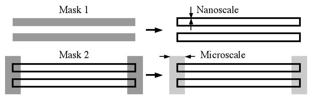
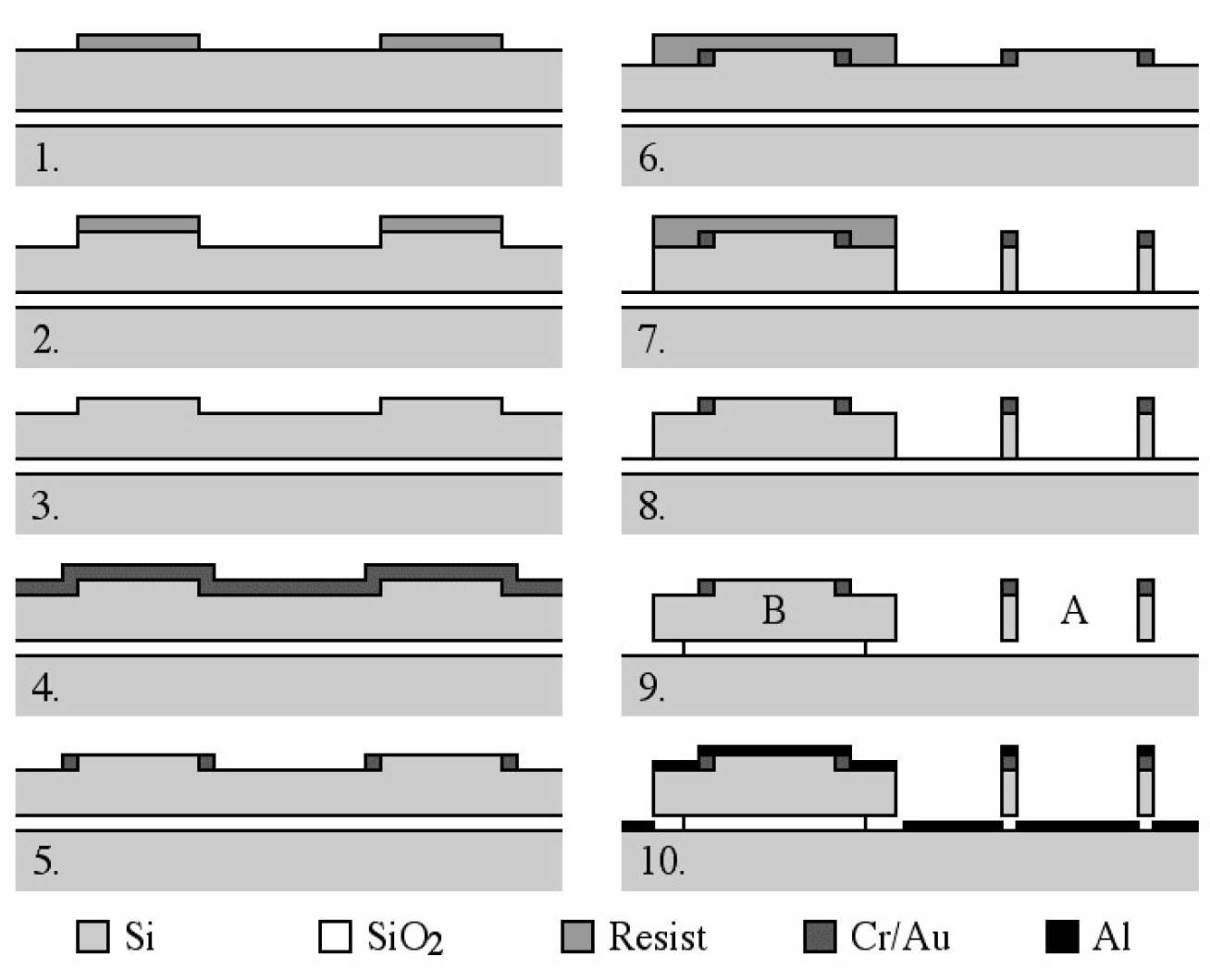
We have developed a batch fabrication process for nano-electro-mechanical systems (NEMS) based on sidewall transfer lithography (STL). STL can be used to form nanoscale flexible silicon suspensions entirely by conventional photolithography. A two-step process for combining microscale and nanoscale features has been developed to fabricate double-ended and single-ended electrothermal actuators with a minimum feature width of 100 nm and a depth of 5 microns, i.e. an aspect ratio of 40 : 1. All devices are fabricated by deep reactive ion etching in 4.5 µm thick silicon using bonded silicon-on-insulator material. The process could allow low cost fabrication of nanoscale sensors and actuators.
Richard Syms and Dixi Liu
We have developed a process to fabricate nano-electro-mechanical systems (NEMS) based on multilayer sidewall transfer lithography (STL). The process uses three pattern transfer steps. Each step only requires optical lithography, making the method suitable for low-cost, wafer scale fabrication. The first two involve STL and are used to form nanoscale features such as suspension beams. These may now intersect, breaking an important restriction of single-layer STL NEMS. The third involves conventional lithography and is used to form microscale features such as anchors. Current nanoscale features have a width of 100 nm and 40 : 1 aspect ratio. The new process should allow mass parallel fabrication of complex NEMS without the need for e-beam patterning.
 |
|---|
| Single-layer STL NEMS process for an example single-axis electrothermal actuator. |
|
|
|---|
| Multi-layer STL NEMS process for example two-axis electrothermal actuator. |

 |
|---|
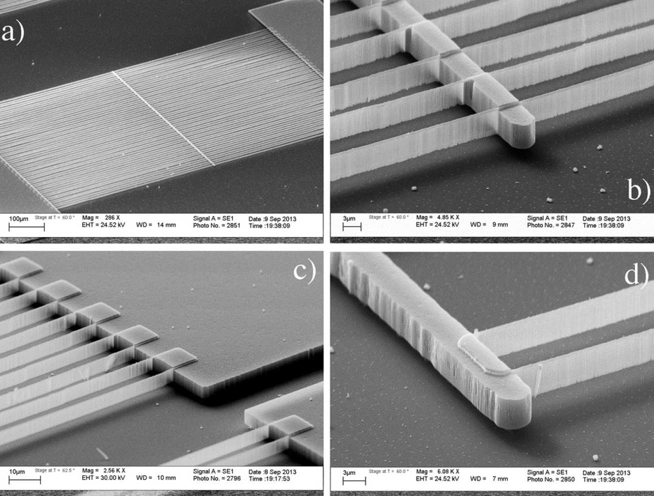
| SEM images of a) etched compound mesa, b) and c) sidewall mask, d) high aspect ratio Si nanostructure. |
 |
|---|
| SEM and interferometric images of crossbeams and electrothermal drive. |
Richard Syms, Dixi Liu and Munir M. Ahmad
We have demonstrated sidewall transfer lithography (STL) as a method for parallel fabrication of 2D nanostructured cellular solids in single-crystal silicon. The linear mechanical properties of four lattices (perfect and defected diamond; singly and doubly periodic honeycomb) with low effective Young’s moduli and effective Poisson’s ratio ranging from positive to negative have been modelled using analytic theory and the matrix stiffness method with an emphasis on boundary effects. The lattices have been fabricated with a minimum feature size of 100 nm and an aspect ratio of 40 : 1 using single- and double-level STL and deep reactive ion etching of bonded silicon-on-insulator. Nanoelectromechanical systems (NEMS) containing cellular materials have been used to demonstrate stretching, bending and brittle fracture. Predicted edge effects have been observed, theoretical values of Poisson’s ratio verified and failure patterns described.
|
|
|---|
| a)-d) SEM views of nanostructured cellular materials with different lattices, formed in single crystal silicon; e) ,f) nanoelectromechanical systems containing cellular materials; g), h) nanostructured materials after bending out-of-plane. |

Mino Green, Elizabeth Fielder, John Stagg - UK
Bruno Scrosati, Mario. Wachtler and Judith Serra Moreno - Italy
An on-chip, integrated lithium battery that can be recharged by an external coil is highly desirable for various medical implants, e.g. of the cochlea. Achieving this goal is the ultimate objective of this work. Silicon has the highest density capacity per unit volume of any of the potential anode materials. The problem is that the insertion of Li into Si (which yields Si5Li22) results in a volumetric expansion of two. Such large volume changes are a major cause of failure. In an EEC sponsored project carried out jointly with the University of Rome, we have shown that nano-structured pillars fabricated by island lithography on silicon wafers can retain their mechanical integrity, even after many cycles of insertion and extraction, because the pillars are mechanically constrained only at their base. This work is being extended, by using inductively coupled plasma etching by the cyclic Bosch DRIE process, to increase the pillar height and hence the charge capacity. Work on the cathode is also planned for the next period.
 |
|---|
| Si nanopillars formed by island lithography and deep reactive ion etching |
 |
|---|
| Structure changes on charge/discharge cycling |
 |
|---|
| Schematic of integrated externally re-chargable Li battery for medical implants |
Kristel Fobelets (EEE), Tim Albrecht (Chemistry), Abdurrahman Shougee (EEE), Foivia Konstantinou (Chemistry) and Lu Qiao (Chemistry)
This project is driven by the wish to combine green energy storage devices and integrated electronics. Supercapacitors or double layer capacitors are attracting a lot of attention because of their high capacitance value and long lifetime. They cannot be used as a continuous power source, though they can be quickly charged and discharged. In many electronic applications this is an attractive feature making integrated supercapacitors a promising research topic.
Si is ubiquitous in the electronics world but is not commonly regarded as a basis for supercapacitors. Our research has therefore focussed on increasing the capacitance of Si-based electrodes by nano-structuration and increasing the chemical stability by cost competitive wet chemistry. The fabrication process and the use of room temperature ionic liquids put these micro-supercapacitors within the green chemistry remit. Our most recent results are obtained by transforming bulk silicon into a forest of 10 m long nanowires, coating them with TiO2 using a wet chemical dip process and using the ionic liquid [Bmim][NTF2]. The best TiO2 coated Si nanowire array electrode in [Bmim][NTF2] showed energy densities of 0.9 Wh·kg-1 and power densities of 2.2 kW·kg-1.
 |
|---|
3 different coating processes were applied. The SEM cross section of the resulting nanowires are shown for the 3 processes. The centre figure is the cyclic voltamogram showing the best result for the 3x dip in Ti(OCH2(CH3)2)4.
Reference
1. F. Konstantinou, A. Shougee, T. Albrecht, and K. Fobelets, “TiO2 coated Si nanowire electrodes for electrochemical double layer capacitors in room temperature ionic liquid”, accepted for publication in Journal of Physics D: Applied Physics (2/8/2017).
Eric Yeatman, Mino Green, Orla McCarthy
The sol-gel technique for depositing glass layers has the peculiar feature that before being fully densified the material is porous on a very fine, i.e. nanometre, scale. We have been investigating ways to exploit this nanoporosity to add new functionality to the material, and to develop new fabrication processes. One way to extend optical functionality is to grow nanocrystalline dopants within the pores. These combine the waveguiding properties of the host glass with the active properties of the crystals, which can be enhanced by quantum size effects. We have fabricated silica-on-silicon waveguides doped with semiconductor crystallites, clearly showing quantum shifting of the band-gap energy, and have measured nonlinear refraction in this waveguides, a process with potential applications in high speed all-optical switching. We have also grown rare-earth containing crystallites, which show fluorescence properties not obtainable in the host glass, and are investigating applications in lasers and optical amplifiers. We have also demonstrated ionic doping of the porous films through a high resolution photoresist pattern, making a low cost new process which can be used for patterned modification of index, softening temperature, or active properties.
 |
|---|
| TEM photograph of CdS semiconductor micro-crystals (black dots) in a silica film. Typical dia is 50A. |
 |
|---|
| Optical microscope photograph of silica film doped with Pb ions using the patterned pore doping method. |
Sam Al-Bader
Advances in nanofabrication and near-field detection techniques have stimulated research into the transmission properties of sub-wavelength waveguides and nano wires. It is desirable to utilize the large bandwidth of light while maintaining the development of miniaturization of electronic elements and devices. One approach that promises size reduction beyond that imposed by the diffraction limit on dielectric components is the use of surface waves particularly plasmon waves for signal transmission. These waves (or modes) can be supported by many metals. Questions that relate to the dispersion, loss, excitation, detection and field confinement are of basic interest to nanofabrication and near-field microscopy. We have studied the fundamental optical modes of a rectangular metallic stripe of sub-wavelength cross-sectional dimensions. The modes shown here are for a silver wire of 1 x 0.1 micrometer embedded in Si at a wavelength of 1.55 micrometers. The outlines of the wire are defined by the overlap of the dark blue strips with the wider dimension along the x-axis.
 |
|---|
| Fundamental lower branch mode, magnitude of the x-directed magnetic field. |
 |
|---|
| Second lowest order lower branch mode. |
 |
|---|
| Fundamental upper branch mode. |
Stepan Lucyszyn and Michael Larsson
The formation of C60 nanowhiskers via the liquid-liquid interfacial precipitation technique presents a low-cost means of fabricating nano-structured fibres for use as active or passive elements in a number of possible applications. Recent measurements by Miyazawa et al. have reported encouraging electrical characteristics that indicate the possibility of using C60 nanowhiskers to realise electronic devices with switching or sensing capabilities. In this work, we focus on one application in particular – millimetre-wave power detectors. Traditional detectors based on Schottky junctions have difficulty impedance matching over very wide video bandwidths, in addition to insensitivity to very low power signals and high susceptibility to thermal and shot noise. C60 nanowhiskers offer the possibility of realising low-cost, robust, sensitive millimetre-wave detectors with significantly reduced shunt capacitance and improved noise performance. Before this can be achieved, however, techniques are needed to control growth parameters and eliminate assembly through in-situ growth. Preliminary experiments have indicated the possibility of using DC electric fields to align C60 nanowhiskers, however, much work is needed to refine the technique to exercise control over growth dimensions and locations.
Related Publications
S. Lucyszyn, M.P. Larsson, K. Miyazawa, J.-J. Tsaur and M. Ryutaro, “Growth of C60AT’s nanowhiskers for quiet millimetre-wave detectors”, Invited paper, CAS ‘05 International Semiconductor Conference, Oct. 3-5, Sinaia, Romania, pp. 9-16, 2005.
Z. A. K. Durrani
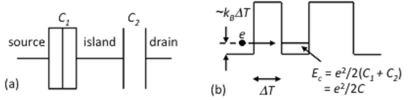
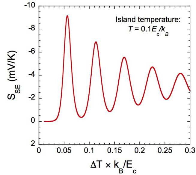
The Seebeck coefficient, S = DV/DT, provides a measure of the thermoelectric effect in a material, where voltage DV is generated by the application of temperature difference DT across the material. Furthermore, as DV depends on the electron transport properties, and DT on the thermal properties of the material, the measurement of S provides information about fundamental charge and heat flow in a material or a device. It is demonstrated theoretically that in a nanoscale island where single-electron charging occurs [1], even one electron on the island can generate a measurable Seebeck effect [2]. Figure 1(a) shows a single-electron box circuit, where an island is tunnel coupled to the source, and capacitively to the drain, and temperature difference DT exits across the tunnel junction. Thermally-excited electrons transfer on to the island only if kBDT > Ec = e2/2C, where Ec is the single-electron charging energy and C the island capacitance (Fig. 1(b)). Increasing DT transfers electrons one-by-one on to the island and leads to an oscillating single-electron Seebeck coefficient SSE (Fig. 1(c)). The peak value of SSE can be very large, ~10 mV/K, suggesting an alternative approach to create an efficient thermoelectric material.
References:
1. Durrani, Z. A. K., Physica E 17, 572 (2003).
2. Durrani, Z. A. K., J. Appl. Phys. 115, 094508 (2014).
Emiljana Krali, Kristel Fobelets, Z. A. K. Durrani
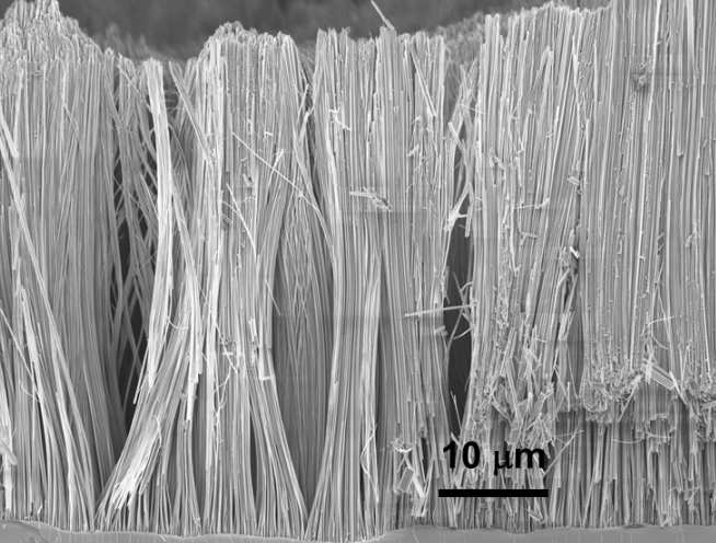
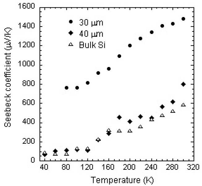
In the last decade, there has been a great interest in thermoelectric effects (TE) in semiconductors for energy recovery and generation. In particular, attention has focused on TE devices based on nanostructured materials [1, 2]. This approach allows the possibility of silicon TE devices, compatible with large-scale integrated circuit fabrication. Silicon nanowires (NWs) may provide a high thermoelectric figure-of-merit ZT = S2σT/~ 1 due to a reduction in the thermal conductivity Here S and T are the Seebeck coefficient, electrical conductivity, and the absolute temperature.
We measure the temperature dependence of S in n-type Si and SiNW arrays, with doping concentration ~1018 cm-3. The Si NW arrays (Fig. 1) were created using a metal-assisted chemical etching (MACE) process [3]. This process produces NW arrays with diameter varying from ~30 – 400 nm and large aspect ratio (up to 1:3000). A transient measurement of voltage ∆V and temperature ∆T, allows characterisation of S = ∆V/∆T. Figure 2(a) shows S measured in n-Si and SiNW arrays, with NW lengths of 30 – 40 μm. S of 30 μm SiNWs is found to be 2.5 times higher than bulk Si at room temperature. Furthermore, of SiNWs is strongly reduced to ~0.2 that of bulk, due to phonon scattering. A best case value of ZT ≈ 0.34 = 55ZTBulk is measured (Fig. 2(b)) [4] .
[1] S. K. X. Bux, J.-P. Fleurial R. B. Kaner, Chemical Communications, 46 (2010)8311 – 8324.
[2] A. I. Hochbaum, R. Chen, R. D. Delgado, W. Liang, E. C. Garnett, M. Najarian, A. Majumdar, P. Yang, Nature, 451 (2008) 163 – 167.
[3] E. Krali, Z. A. K. Durrani, Applied Physics Letters, 102 (2013) 143102-1–143102-4.
[4] Krali, E., Fobelets, K., Durrani, Z. A. K. (2014). ‘Seebeck Coefficient in Si Nanowires and Single-Electron Effects’, 40th Int. Conference on Micro and Nano Engineering (MNE2014), 22 – 26 Sept., Lausanne, Switzerland.
Zahid Durrani, Emiljana Krali, and Mervyn Jones
Semiconductor suspended nanowire (NW) structures are of great interest in a wide range of nano-electromechanical resonator applications. These structures form promising building blocks for nanoelectronic sensors with ultra-sensitive mass detection resolution towards the single-molecule level, for highly efficient thermoelectric ‘clean’ energy generation, and for quantum computation. These nanostructures are also of great interest for investigations of fundamental electrical, mechanical and material properties at reduced dimensions.
The incorporation of nanocrystals within suspended NW structures provides a mean to measure interactions of single electrons and phonons in zero-dimensions, as these are confined within cavities formed by the suspended nanocrystals. These interactions occur for low energy acoustic phonon-like modes, allowing measurement of this part of the phonon spectrum and providing a complementary technique to conventional methods such as Raman spectroscopy
In collaboration with CSIC Barcelona, Spain, a suspended p-type Si NWs incorporating nanocrystals, with an adjacent electrostatic gate, has been operated as a single-hole transistor (Fig. 1(a)) [1]. This enabled measurement of the interaction between single holes and acoustic phonons in the nanocrystals. Devices were fabricated using a novel fabrication process based on focused gallium ion beam exposure and wet etching, creating <10 nm nanocrystals within narrow suspended Si NWs. Electrical characteristics at 10 K consisted of well-defined Coulomb diamonds associated with a single dominant nanocrystal (Fig. 1(b)). These diamonds were split into two regions, due to the lifting of the Coulomb blockade by a ~7 meV acoustic-phonon mode in the nanocrystal. The results corresponded well to Raman measurements on nanocrystals and demonstrated an alternative, electrical means to measure their phonon modes.
Reference
[1] ‘Resonant tunnelling features in a suspended silicon nanowire single-hole transistor’, Jordi Llobet, Emiljana Krali, Chen Wang, Jordi Arbiol, Mervyn E. Jones, Francesc Pérez-Murano, Zahid A. K. Durrani, Applied Physics Letters Vol. 107, 223501 (2015)
 |
|---|
Zahid Durrani, Chen Wang, and Mervyn Jones
During the last 40 years, the Si metal-oxide-semiconductor field effect transistor (MOSFET) has been the driving force of the semiconductor revolution. Scaling the dimension of the smallest physical features within the MOSFET, from micrometres to close to 10 nm, has enabled significant increases in the number of devices per chip, and a corresponding increase in its performance, with greater speed and decreased power consumption. However, the MOSFET remains a device operating according to the principles of classical physics, and at the sub-10 nm to the few-nanometer scale, quantum-mechanical effects and statistical charge fluctuations prevent device operation. Furthermore, the fabrication of these devices by optical lithographic techniques even at the shortest wavelengths greatly increases the process complexity and hence cost.
Advanced lithographic and nanofabrication methods provide a means to fabricate devices towards the few nanometer scale. Nanolithographic techniques such as high-resolution electron beam lithography (EBL), and more novel methods such as scanning probe lithography (SPL), provide a means to define device features at the 10 nm scale, and are particularly suitable for device prototyping, and for investigations of advanced quantum-effect device structures such as single-electron transistors, quantum dots, and quantum computation devices. In combination with nanofabrication methods such as controlled oxidation and etching, it is possible to obtain devices where the electronic core is <5 nm in size, or consists of a single dopant atom. As part of the EU ‘Single Nanometer Manufacturing’ programme, we have developed the use of EBL and SPL methods and have obtained single-electron and quantum dot transistors with cores down to ~1.6 nm in size. This work was conducted as part of a close collaboration with the Technical University of Ilmenau (TUIL), Germany, IBM Zürich, and Swiss Litho, both in Switzerland for SPL based nanofabrication. Figure 1 shows ‘point-contact’ quantum dot transistors capable of room temperature operation, fabricated by EBL (Fig. 1(a), SEM image) [1] and by SPL [2] methods (Fig. 1(b), SEM image of device fabricated in collaboration with IBM, and Fig. 1(c), AFM image of device fabricated in collaboration with TUIL). The device structures are fabricated in silicon-on-insulator material, and reactive ion etching is used for pattern transfer. Oxidation of the ~10 nm wide point contacts allows isolation of a single sub-5 nm scale nanocrystal, or a single dopant atom, within the point contact. These devices illustrate the feasibility of advanced nanofabrication methods for few-nanometre size electronic devices for future quantum effect electronics applications.
References:
[1] ‘Excited states and quantum confinement in room temperature few nanometre scale silicon single electron transistors’, Z. Durrani, M. Jones, C. Wang, D, Liu, J, Griffiths. Nanotechnology Vol. 28, 125208 (2017).
[2] ‘Pattern-generation and pattern-transfer for single-digit nano devices’, Ivo W. Rangelow, Ahmad Ahmad, Tzvetan Ivanov, Marcus Kaestner, Yana Krivoshapkina, Tihomir Angelov, Steve Lenk, Claudia Lenk, Valentyn Ishchuk, Martin Hofmann, Diana Nechepurenko, Ivaylo Atanasov, Burkhard Volland, Elshad Guliyev, Zahid Durrani, Mervyn Jones, Chen Wang, Dixi Liu, Alexander Reum, Mathias Holz, Nikolay Nikolov, Wojciech Majstrzyk, Teodor Gotszalk, Daniel Staaks, Stefano Dallorto, and Deirdre L. Olynick. Journal of Vacuum Science & Technology B 34, 06K202 (2016).
 |
|---|
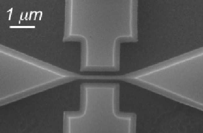
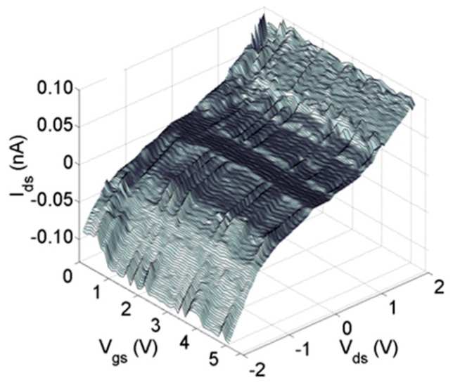
Silicon nanowires (SiNWs) are highly promising materials for nanoscale field-effect transistor, molecular sensor, solar-cell and thermoelectric applications. SiNWs may be prepared by ‘bottom-up' material synthesis techniques such as vapour-liquid solid growth, or by ‘top-down' high-resolution lithographic techniques. It is also possible to prepare SiNWs by a metal-assisted chemical etching (MACE) process [1-2], without the need for complex lithographic or epitaxial techniques.
The MACE process allows for the rapid, low-cost fabrication of large numbers of long (~300 μm) NWs. Etching of a Si wafer in a HF/AgNO3 solution leads to an array of SiNWs via an electrochemical ‘redox' reaction. The arrays consist of vertical NWs with packing density ~109 /cm2 (Fig. 1(a)). Transmission electron microscopy shows that the NWs consist of a ~30-200 nm diameter crystalline core, covered by amorphous shells (Fig. 1(b)). The NW diameter/length ratio is extremely high, up to 1:1500. FETs may be fabricated using individual NWs, dispersed onto a SiO2-on-Si wafer (Fig. 2) [1]. The IDS-VDS and IDS-VBG characteristics for a SiNW p-FET, using the underlying substrate 'back-gate' voltage VBG, are shown in Fig. 3(a) and Fig 3(b) respectively. The field-effect hole mobility μh ~ 100 cm2/V.s, with peak transconductance gm ~ 30 ns.
 |
|---|
| Figure 1 |
 |
|---|
| Figure 2 |
 |
|---|
| Figure 3 |
[1] M. Zaremba-Tymieniecki, Chaunbo Li, K. Fobelets, and Z.A.K. Durrani, IEEE Electron Device Lett. 31, 860 (2010).
[2] K. Fobelets, P. W. Ding, N. Mohseni Kiasari, and Z. A. K. Durrani, ‘Electrical transport in polymer covered silicon nanowires', Field-effect transistors using silicon nanowires prepared by electroless chemical etching', IEEE Trans. on Nanotechnology 99, 1 (2010).
Chen Wang, Mervyn Jones, Zahid Durrani
New approaches to device design, lithography and fabrication of nanoelectronic CMOS devices may be required at the sub-5 nm scale and beyond. Successful ‘beyond CMOS’ technology presents a far greater technological challenge, where a transition may be possible to quantum-effect devices with scaling in all three dimensions to < 5nm, e.g. single-electron transistors (SETs) and quantum-dot (QD) based devices. Unlike ‘classical’ devices, these devices inherently tend to improve in performance with size reduction, thus encouraging continuing development. One potentially important device structure at these dimensions is the single electron transistor (SET) [1], [2].
We fabricate SETs based on Si nanowires (NWs), which have been heavily doped n-type, then oxidized. Device current was controlled using dual in-plane side gates. The devices were defined in silicon-on-insulator (SOI) material using electron beam lithography (EBL) (Figure 1). NWs with two different gate lengths of 1μm and 50nm, have been measured. The SETs were measured from 8 - 300 K with single-electron operation established from 8 K to ~300 K [3]. A ‘Coulomb staircase’ occurs in the drain-source current (Ids) vs. drain-source voltage (Vds) characteristics, Figure 2 (See Ref. 3). Near threshold, the variation in the NW potential due to the disorder and pattern-dependent oxidation creates charging ‘islands’ isolated by tunnel barriers, forming the SETs. Changing the shape of the side-gates can change the configuration of the islands/tunnel barriers controlled by the gate voltage. Single-electron Monte Carlo simulations may be used to explain the details of these SET characteristics through the formation of a multiple-tunnel junction (MJT) along the Si NWs.
[1] Y. Takahashi, Y. Ono, A. Fujiwara, and H. Inokawa, J. Phys. Condens. Matter 14, pp. 995–1033, (2002).
[2] Z. A. K. Durrani, ‘Single-electron devices and circuits in silicon’, Imperial College Press, London (2010).
[3] Chen Wang, M. E. Jones, Z. A. K. Durrani, Nanotechnology Vol. 26, p305203 (2015).
Kristel Fobelets, Pei Wern Ding, Jesus-Enrique Velazquez-Perez (Univ. Salamanca)
The novel and innovative screen-grid FET (SGFET) is an example of an independent-multi-gate thin Si film FET (SOI) architecture and is seen as the potential competitor of finFETs. The SGFET - named as in the tetrode (vacuum tube technology) is shown in the top figure with two rows of gating fingers. The main difference between the SGFET and all other semiconductor FET structures is the geometrical relationship between the gate and the channel connecting the source with drain. As the figure shows, the gating fingers are perpendicular to the current in the channel and gating acts radially from the gate cylinders into the channel. This geometry disconnects the relationship between the dimensions of the gate and the source-drain distance. The gate length in the SGFET can be seen as the distance between 2 gate fingers within one row. The SGFET belongs to the league of multiple gated FETs (MugFETs) where the channel between two gate cilinders within one row is enhanced or depleted via double gating action. The second gate finger row, nearer to the drain, acts to screen the influence of the drain voltage on the source as in the tetrode. The screen-grid FET allows downscaling without increasing output conductance, nor increasing parasitic capacitance nor decreasing mobility. Initial simulations indicate that for optimum operation an undoped channel layer is needed, thus also allowing maximum mobility, minimum noise and a possibility of ballistic transport. Moreover the double-row gate finger configuration is the ultimate solution for DIBL control while retaining an excellent gm/IDS figure of merit. As for finFETs, the threshold voltage in the SGFET is controlled by selecting an appropriate gating metal.
 |
|---|
| Schematic configuration of embedded-gate 3D nano-FET. Top: 3D side view, bottom: channel region only. Dimensions of the geometry of the SGFET is in the nanometer range. |
 |
|---|
| Figure of merit “gm/Ids” for Vds=100mV. Red: 1 row gate configuration, green: 2 row gate configuration |
Z. A. K. Durrani
Y. T. Tan, M. A. H. Khalafalla (University of Cambridge)
H. Mizuta (University of Southampton)
Nanocrystalline silicon (nc-Si) thin films, where crystalline silicon grains ~10 nm in size are separated by narrow amorphous silicon or silicon oxide grain boundaries (GBs), inherently form a material system consisting of arrays of silicon quantum dots. These films provide a means of using ‘bottom-up’ growth techniques to define large numbers of nanoscale quantum dots, without high resolution lithography. In this work, we fabricate single-electron transistors (SETs) operating at room temperature in ~20 nm-thick nc-Si thin films (Fig. 1). The films contain crystalline silicon grains ~10 nm in size, separated by SiOx grain boundaries. In SETs with small 20 nm20 nm channels and only a single dominant grain, single-electron current oscillations are observed at room temperature (Fig. 2), raising the possibility of the practical application of SETs. In SETs with larger channels containing more than one grain, electrostatic and electron wavefunction coupling effects (‘quasi-molecular’ states) are observed at 4.2 K (Fig. 3), adjacent grains forming coupled quantum dots.

Zahid Durrani, Chen Wang, Dixi Liu, and Mervyn Jones
As the minimum size of semiconductor electronic devices is reduced to the ~10 nm, increasingly challenging barriers are being encountered in both device physics and technology. In any successor ‘beyond CMOS’ technology at the sub-10 nm scale, quantum mechanical effects are increasingly likely to influence the behaviour of the component nanoelectronic devices, raising the possibility of advanced devices operating according to the principles of quantum physics. Developing quantum electronics into a practical technology requires devices at the single-nanometre scale, which can both operate at room temperature (RT) and are manufacturable. Single nanometre scale quantum dots (QDs) have great potential in this regard, for applications in nanoelectronic circuits, quantum computation, single molecule sensing, and energy scavenging. QD transistors are particularly attractive because, unlike ‘classical’ transistors, a reduction in size inherently improves their performance. Quantum dots can now even be defined by a single donor atom, of great interest for quantum computation devices.
We have demonstrated single-electron quantum dot (QD) transistors, with QD size down to <2 nm and operating at room temperature (RT = 290 K) [1-2]. Point-contact transistor structures (Fig. 1(a) and (b)) were fabricated in heavily doped n-type SOI wafers with an ultra-thin (12 nm) top Si layer. The devices were defined by using high-resolution electron beam lithography (EBL) and reactive ion etching, combined with a geometry dependent controlled oxidation process to isolated a few-nanometre scale QD in the point-contact (Fig. 1(a)). Full QD operation at RT was observed in multiple devices, including measurement of both charging and excited quantum confinement states (Fig. 1(c) and (d)), the later effect for the first time at RT. A remarkably large QD electron addition energy Ea ~ 0.8 eV = 30 kBT at 290 K, the largest reported, was obtained. Here, the quantum confinement energy ~0.3 eV, implying the formation of a QD only ~1.6 nm in size. The likely origin of the QD was a potential well formed by a donor atom embedded in the thin SiO2 region formed by geometric oxidation of the point-contact neck.
References
1. ‘Excited states and quantum confinement in room temperature few nanometre scale silicon single electron transistors’, Durrani, Z, Jones, M, Wang, C, Liu, D, Griffiths, J, Nanotechnology 28, 125208 (2017).
2. ‘Fabricating single electron devices in silicon for room temperature operation using electron beam lithography and geometric oxidation’, Chen Wang, Dixi Liu, Jon Griffiths, Mervyn Jones, Zahid Durrani, MNE2016, Vienna 19 – 23 Sept. (2016).
 |
|---|
Christoforos Panteli, Oleskiy Sydoruk, Kristel Fobelets
We have explored the use of sensors based on graphene on etched silicon nanowire arrays (GrNWA). The wire fabrication process involves nucleating silver nanoparticles on a Si substrate in HF and using these as a surface mask to etch high aspect ratio structures using H2O2 in HF. The nanowire diameter is 50-250 nm and their spacing 200 nm. The graphene layers are then added using a layer transfer process. The starting material is graphene on a nickel-coated, oxidised Si substrate. A layer of PMMA is first spin coated to provide a mechanical support. The Ni layer is then removed using a nickel etchant, so that the graphene detaches. Graphene is then transferred to the silicon nanowire array and the PMMA is removed using acetone vapour. SEM images show graphene appearing as a thin layer on top of the nanowires. The same process can be used to transfer graphene onto SiO2 (GrOx) and O2 pre-treated Si (GrSi) substrates. We have used these structures for ammonia sensing, by monitoring resistivity with a four-point probe. Experimentally, we find that GrNW reacts 8 times more and 16 times faster than GrOx and recovers 44 times faster. Therefore, graphene suspended on SiNWAs significantly enhances gas adsorption. The universal layer transfer process can be used to realize suspended graphene and improve the performance of other graphene-based gas sensors.
 |
|---|
| Nanowire fabrication process. |
 |
|---|
| Graphene transfer process. |
 |
|---|
| SEM images of graphene on nanowire arrays. |
 |
|---|
|
Comparison of ammonia vapor responses for graphene on nanowires, silicon and oxide. |
Faris Abualnaja, Mervyn Jones, Zahid Durrani
Single-dopant atom quantum dot (QD) transistors are single-electron devices where charge is stored on potential wells created by impurity atoms within a semiconductor or insulating silicon matrix. An electrostatically coupled gate terminal may be used to control electrons held within these wells and allow current to be switched ‘on’ or ‘off’, creating atomic scale transistor and memory devices. Previous to our work, these devices had been defined using dopant atom QDs in semiconductors such as silicon, where the very shallow potential well (~10 meV) limited electron trapping to cryogenic temperatures. However, we have shown that impurity atoms embedded within a ~10 nm scale SiO2 tunnel barrier allow QDs with very deep potential wells (~1 eV) to form [1-2], increasing the operating temperature to room temperature (RT) and raising the possibility of practical, large scale integrated circuit applications. Furthermore, in dual gate devices, it is possible to observe electrostatic interactions between these QDs, leading to double quantum dot (DQD) or diatomic molecule-like behavior [2].
DQD transistors were fabricated using ~10 nm scale point-contact transistor structures in heavily doped n-type (phosphorous doping) silicon-on-insulator (SOI) material. The point-contact transistors were defined using electron beam lithography and controlled oxidation. RT measurements (Fig. 1) show current peaks which define hexagonal ring patterns (Fig. 2) at specific gate voltages. The hexagonal rings are signatures of series coupled DQDs, where the electron number (N1, N2) on the two QDs is constant within the ring. The current peaks and the patterns they define can be extracted automatically using image recognition methods based on Otsu’s algorithm for thresholding and the Hough Transform for circle detection (Fig. 2).
[1] Z. A. K. Durrani, M. Jones, F. Abualnaja, C. Wang, M. Kaestner, S. Lenk, C. Lenk, I.W. Rangelow, and A. Andreev, Journal of Applied Physics 124, 14 (2018) 144502.
[2] F. Abualnaja, C. Wang, V-P Veigang-Radulescu, J. Griffiths, A. Andreev, M. Jones, Z. Durrani, Phys. Rev. Appl. 12, 064050 (2019).

|
Figure 1. RT measurements of DQD characteristics. Complete and partial hexagonal patterns (1-5) are marked by solid red and dashed white lines as detected by image processing methods. |
Figure 2. Image processing program applied to Vgs1 = 0.5 to 2 V and Vgs2 = 1.2 to 2.5 V (a, b) and Vgs1 = 2 – 3.2 V and Vgs2 = 0.8 – 1.8 V (c, d). |