The end of Moore's Law?
Jim Greer is a Professor in Advanced Electronic Materials and Devices at the University of Nottingham’s Ningbo Campus, China.
Microchips have made computers, smart phones, and the internet possible, which has revolutionised how we work, shop, travel, and socialise.
Moore's Law specifies that the number of transistors in an integrated circuit will double every two years, which has allowed the development of the personal computer, smart phone and much more consumer electronics. The Law is named after former CEO of Intel Gordon Moore, who published his prediction in 1964 and has held remarkably accurately until modern times.
Transistors at the atomic scale
The way we live, socialise and communicate is a consequence of these technological developments. This is just 50 years of development, compared to 6000 years of written history - there's a lot of development still to come! Professor Jim Greer Professor in advanced electronic materials and devices, University of Nottingham, Ningbo Campus, China
For Moore's Law to continue, circuits must keep getting smaller and smaller. In 2012, a transistor was on the scale of 3 nanometre, about the width of 6 silicon atoms. Today it is at single atomic widths. At such atomic scales, we get quantum mechanical effects such as quantum tunnelling. Here, electrons go through the insulating layers, so the switch in the circuit cannot be off. Therefore the question is: how can Moore's Law continue and electronic circuits keep getting smaller?
In his IMSE Highlight Seminar, Professor Greer's described that, so far, solutions have involved designing new types of materials. However finding an appropriate material has taken about 10 years.
The nanowire transistor
One solution outlined in Professor Greer's seminar was a new design of transistor: the so-called nano-wire transistor. The "Junctionless" nanowire transistor, developed at the Tyndall National Institute in Ireland, is a nanowire-based transistor that has no gate junction. Junctions are difficult to fabricate, and, because they are a significant source of current leakage, they waste significant power and heat. Eliminating them holds the promise of cheaper and smaller microchips.
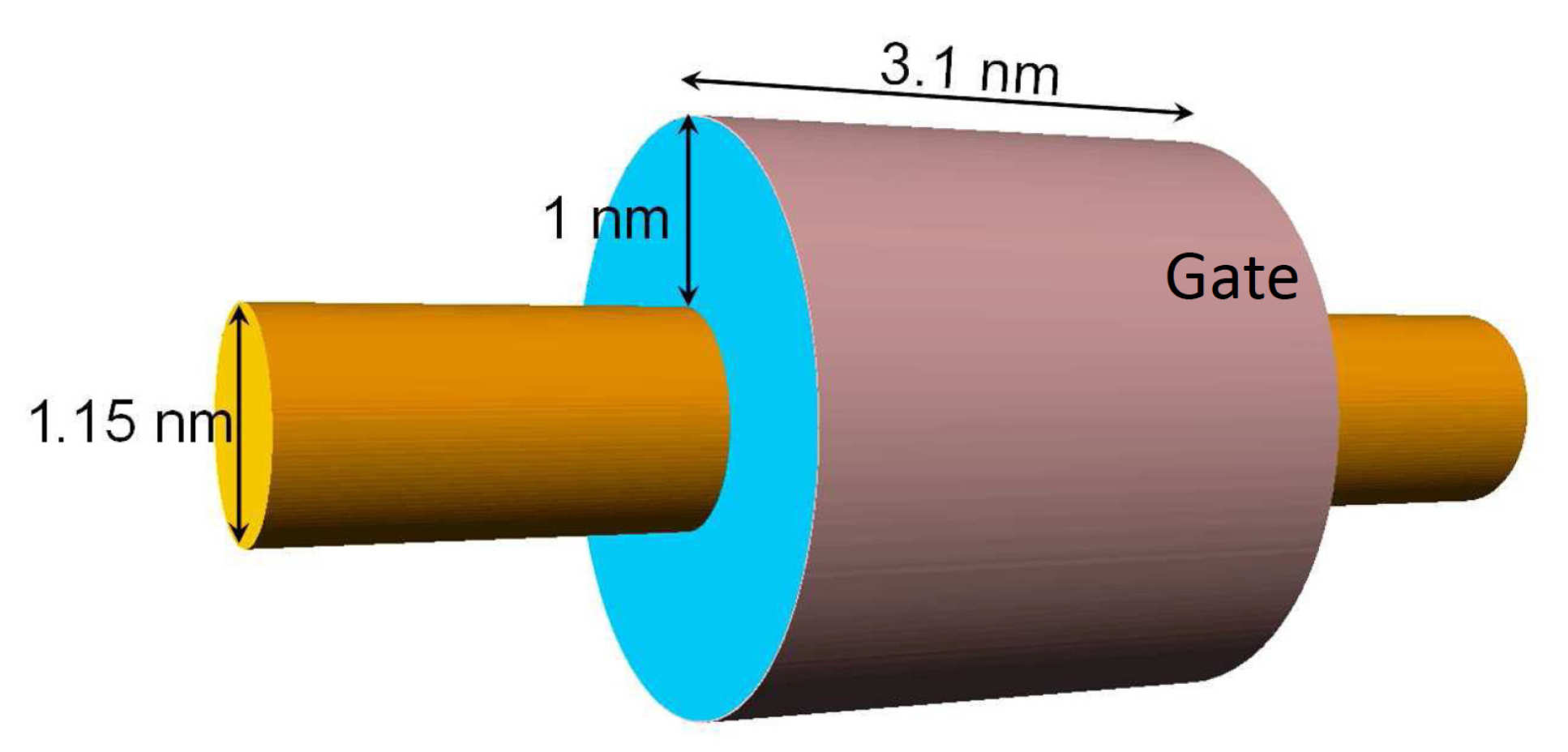
The functionless nanowire transistor uses a simple nanowire of silicon surrounded by an electrically isolated "wedding ring" gate that forces the flow of electrons through the wire, akin to squeezing a garden hose to gate the flow of water through the hose. The nanowire is heavily n-doped, making it an excellent conductor. Crucially the gate, comprising silicon, is heavily p-doped and its presence depletes the underlying silicon nanowire thereby preventing carrier flow past the gate.
However, new manufacturing challenges still exist for these junctionless devices. Although in theory it physically works, according to Professor Greer, it is very difficult to make.
Looking to the future, Professor Greer predicted that to continue the insatiable need for more transistors, transistors would be stacked on top of each other. However a potentially much greater leap in computing power could be in quantum computing. This works because a quantum logic statement doesn’t have one “true” or “false” condition. The answer can be a combination of possible outcomes. Hence many different possibilities can be considered simultaneously.
One possible explanation for why quantum computers work involves parallel universes. It has been theorised that qubits are able to exist in two states simultaneously because we are observing them in multiple universes simultaneously. Now that's just weird.
Article text (excluding photos or graphics) © Imperial College London.
Photos and graphics subject to third party copyright used with permission or © Imperial College London.
Reporter
Dr Kieran Brophy
Faculty of Engineering