What is that?
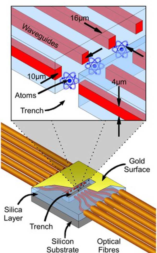
Optical waveguide chips are circuit boards for photons. That's why they are made of glass instead of copper. The conducting paths in that glass chip are regions with slightly different refractive index than its surrounding. Along these paths light is guided, just as in optical fibres. Waveguide chips are already in use in telecommunication networks, processing the data that is send around the world through optical fibres. But not only on commercial scales have those waveguide chips become an important tool. Also in fundamental photonic research experiments with such chips have shown promising results for their application in quantum information processing (QIP). So we are doing the step from a wire to a circuit board for optical access in atom optic experiments.
So that's the photons, but what about the atoms? Our waveguide chip is the first that is used to probe cold atoms. To control the atoms the chip is glued onto a copper sub chip and integrated into a vacuum chamber. The copper chip contains wires that produce magnetic fields when current is run through them. Atoms can interact with these fields, and in the correct field geometry they can be trapped and moved around. And we want to move them into a trench that cuts the waveguides right in the centre. So the light will exit the waveguide on one side of that trench, interact with the atoms in the trench and then couple back into the waveguide on the other side. The atoms will change the way the light propagates, so analysing the light at the output will tell us something about the small cloud of atoms in the trench. And since the light also influences the atoms, we can poke them in a very controlled way and see what happens. The advantage of our experiment compared to most others is that the interaction regions are very well localised within the atomic clouds. And that increases the probability for a single photon to interact with an atom. Since all this happens on an optical circuit board at up to twelve different light-atom interaction points the whole device is scalable, meaning it can be integrated in a larger and more complicated circuit. That's why we call it an atom-photon junction.
Further info
The high probability of photons interacting with the atoms and the large efficiency of collecting these photons after the interaction allows for measuring very cold atomic clouds without disturbing them to much. In most atom optics experiments, information about the state of the atom is gained by looking at a light beam send through the atoms, and counting the photons that are scattered by the atoms. But since the cold clouds are very sensitive to any sort of disturbance, the sample is destroyed each time information is read out. However, since we can very precisely control the number of photons send to the cloud and efficiently collect the photons that have interacted with the cloud afterwards, we have a chance of measuring the atoms without destroying the whole cloud. We will further reduce the effect on the atoms by using light that is detuned from the atomic resonance. This light will not primarily be scattered but rather gather a shift in phase as it would do in a material of a different refractive index than air. Measuring this phase shift instead of photon scattering increases our chance of getting a good measurement without destroying the cloud.
And in QIP? Now, small quantum circuits have already been realised on photonic chips. But they can only process the information. For storing those information, a less volatile quantum system than photons has to be used. For example, atoms trapped inside such a chip ...
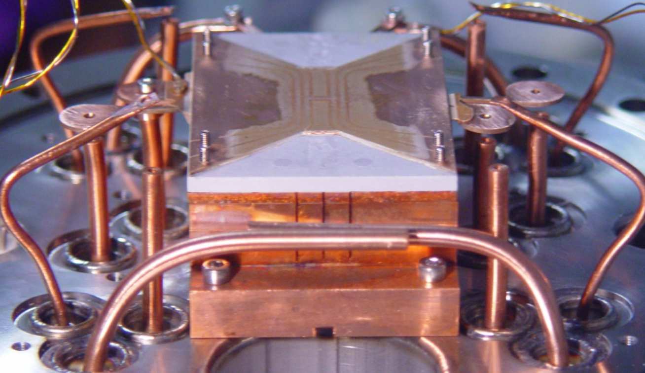
In cooperation with the Centre For Integrated Photonics (CIP) in Ipswich, UK, we have designed and build a silicon-on-silica waveguide chip, containing twelve parallel waveguides with a light field mode of 2.1 µm (1/e electric field radius), intercepted orthogonally by a trench of 16 µm width and 22 µm depth. In that trench, adjacent waveguides have a pitch of 10 µm fanning out to 250 µm to be connected to bundles of single-mode fibres in a commercially available V groove assembly. This allows for supplying individually tailored light to each of the twelve waveguides, for measurement and manipulation of atoms inside that trench. Atoms, in our case 87Rb can be guided and hold inside that trench with magnetic fields, created by a wire subchip. The maximal trap frequencies achievable at the position of the trench (500 µm from the wire surface) with the design current of 50 A are 1100 x 30 Hz.

Our experiment aims at studying dynamic processes in ultra cold atomic clouds. The individual control over the light in each waveguide allows for using them at will for either absorption measurements, resonant fluorescence observation, off-resonant phase-shift detection, conservative optical-dipole potentials or 2-photon coherent manipulation. Combining atomic clouds with integrated waveguide chips may therefore serve as a powerful tool in investigating the few particle quantum nature of trapped particles, spectroscopic measurements or even quantum information processing.
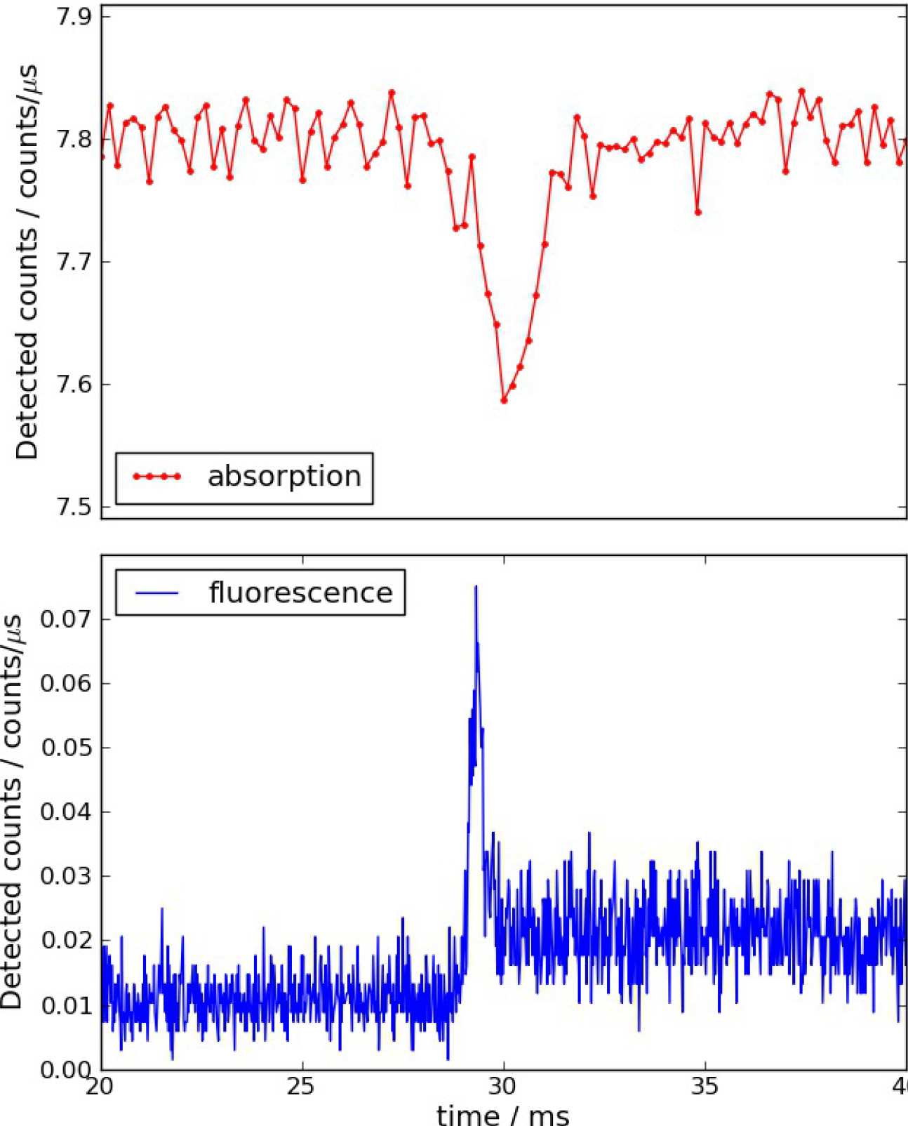 We have already characterised the light-matter interaction on our combined magnetic/optical atom chip with spectroscopic experiments on a cloud of atoms released from a magneto-optical trap (MOT) arXiv:0912.4460
After improving the experiment we are now setting up a (non-destructive) phase measurement on magnetically trapped atoms. For this purpose we will employ light that is frequency modulated around the atomic resonance, but contains no carrier frequency to avoid heating of the atomic cloud by resonant photon scattering. The light interacting with the atoms will therefore contain two frequencies shifted around the resonance by equal amounts but with opposite sign. The relative phase of the beat between the two frequencies after passing the atomic cloud can then be compared to the phase of a local oscillator. The additional phase shift of the light with respect to that local oscillator will then be proportional to the atomic column density at the interaction point. This will allow for real time, local, density measurements with only small perturbation of the atomic ensemble.
"An array of integrated atom–photon junctions", Nature Photonics 5, 35–38 (2011)
"Minimally-destructive detection of magnetically-trapped atoms using frequency-synthesised light", arXiv:1104.0236
"Prospects for using integrated atom-photon junctions for quantum information processing", arXiv:1105.0870
Rob Nyman (r.nyman@imperial.ac.uk), Plamen Petrov, Mattias Kohnen and James Garvie-Cook. If you have further questions or comments or are interested in joining our team, please contact us. We look forward to hearing from you!