Background and motivation
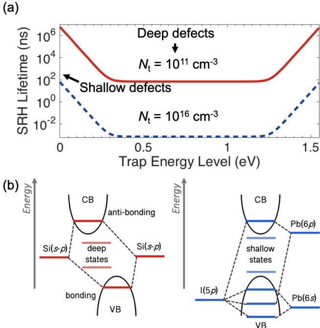
PV materials absorb light to generate electrons and holes. These need to be extracted but can be irreversibly lost via defects. Defects introduce energy levels (traps) in the band gap that annihilate carriers through Shockley-Read-Hall (SRH) recombination. Carefully manufacturing the semiconductor to reduce the defect density is one way to reduce the SRH recombination rate so that photo-generated carriers live long enough to be extracted. A lifetime of at least 1–100 ns is needed for PVs. But SRH also depends on the trap energy level in the band gap. Defects that are close to the band-edge (i.e., shallow) give lower SRH rates and is one way to enable defect tolerance, where a long lifetime is achieved despite a high defect density (Fig. 1a).
Methylammonium lead iodide perovskite has recently been found by serendipity to be defect tolerant. Made by cheap solution processing, these materials have a high trap density of 1015–1016 cm-3 (cf. 108 cm-3 for silicon), but still achieve long SRH lifetimes >100 ns, with devices already outperforming multicrystalline silicon. Defect tolerance has also been found in other lead-halide perovskites, as well as copper indium diselenide. However, safety concerns over the soluble toxic lead content in perovskites may limit their deployment, whereas indium has high cost and limited supply. It is therefore critical to significantly expand upon the classes of defect-tolerant materials well beyond the limited range currently available to fulfil the urgent need for efficient, low-cost PV.
Recent results and examples of defect tolerant materials found
Recently, it has been proposed that ns2 compounds could replicate the defect tolerance of the lead-halide perovskites. These compounds have a partially-oxidised heavy metal cation with a lone pair of valence electrons (e.g., Bi3+, In+ or Sb3+). This is because (1) the valence s2 electrons can hybridise with the anion p orbitals to replicate the perovskite electronic structure, (2) there is large spin-orbit coupling, resulting in disperse bands and shallower defects, and (3) the large electron cloud leads to high polarizability, resulting in a high dielectric constant to Coulombically screen charged defects. Point (1) is especially important. In traditional materials (e.g., silicon), when atomic orbitals overlap, bonding-antibonding orbital pairs form across the band gap (Fig. 1b). When these bonds are broken due to defects, the dangling bonds form close to where the original atomic orbitals were, leading to deep defects. By contrast, lead-halide perovskites form bonding-antibonding orbital pairs in the valence band, as well as across the band gap (Fig. 1b), and dangling bonds then form defects in the valence band or close to the band-edges, resulting in most defects being shallow rather than deep.
Hundreds of materials, containing ns2 cations, have been proposed as having the potential to be defect tolerant. We and colleagues at MIT recently grew six of these materials and showed their charge-carrier lifetimes to be promising for photovoltaic applications (Chem. Mater., 2017, 29(11), 4667-4674). Examples include methylammonium bismuth iodide, antimony sulfoiodide and bismuth oxyiodide.
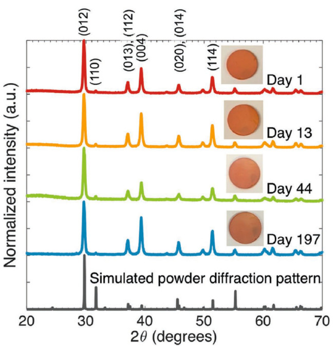
We have particularly investigated bismuth oxyiodide (BiOI) in depth. Bismuth-based compounds have demonstrated very little evidence of toxicity, bismuth is sufficiently abundant for commercialisation in solar cells, and we recently showed BiOI to be air-stable (Fig. 2). We developed an all-inorganic device structure, from which we achieved high external quantum efficiencies that reached up to 80% at 450 nm wavelength, exceeding previous reports of bismuth-based absorbers at the time of publication in 2017 (Adv. Mater., 2017, 29, 1702176). Through computations of the defect diagrams, we found that the dominant point defects in BiOI have shallow transition levels and the material itself to have a high dielectric constant of 45. We followed this up with systematic measurements that showed the electronic structure and optoelectronic properties of BiOI to tolerate percent-level surface defects (Adv. Funct. Mater., 2020, 30(13), 1909983). This experimental evidence is consistent with defect tolerance and is in strong contrast to traditional covalent semiconductors.
Key literature
Review papers
Yi-Teng Huang, et al. Perovskite-Inspired Materials for Photovoltaics and Beyond - From Design to Devices. Nanotechnology, 2021, 32(13), 132004. Highlighted in Nature Physics
Robert L. Z. Hoye,* et al. The Role of Dimensionality on the Optoelectronic Properties of Oxide and Halide Perovskites, and their Halide Derivatives. Advanced Energy Materials, 2021, 2100499, Early View. DOI: 10.1002/aenm.202100499
Research papers
Robert L. Z. Hoye, et al. Strongly Enhanced Photovoltaic Performance and Defect Physics of Air‐Stable Bismuth Oxyiodide (BiOI). Advanced Materials, 2017, 29, 1702176. Press release
Riley E. Brandt, et al. Searching for “defect-tolerant” photovoltaic materials: combined theoretical and experimental screening. Chemistry of Materials, 2017, 29(11), 4667-4674.
Tahmida N. Huq,† Lana C. Lee,† ..., and Robert L. Z. Hoye. Electronic Structure and Optoelectronic Properties of Bismuth Oxyiodide Robust against Percent‐Level Iodine‐, Oxygen‐, and Bismuth‐Related Surface Defects. Advanced Functional Materials, 2020, 30(13), 1909983.
†Equal contribution