We have a decade-long experience in the development of cost-effective synthesis methods, of solution processed graphene and other 2D materials. This enabled the synthesis of high-quality inks and dispersions of conducting, semimetal, semiconducting and insulating 2D materials for high-performance electronics and photonics. The ink formulation is achieved by high-quality and high-yield liquid phase exfoliation process via ultrasonication and electrochemical exfoliation routes, to achieve a wide range of tunability of the morphology 2D and few-layer materials, while microfluidic exfoliation is used to process high volume and loading.
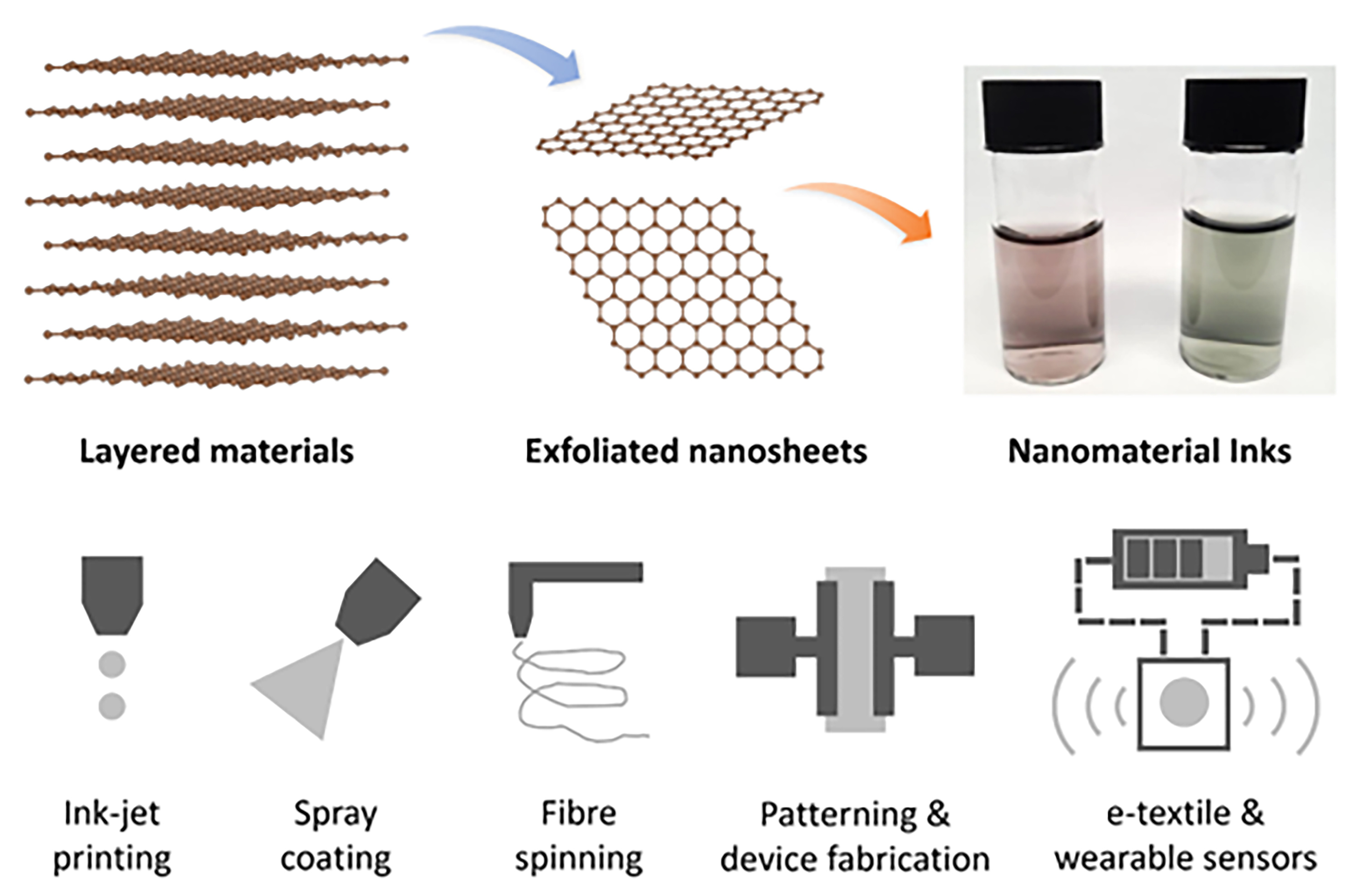
The functional 2D material inks are employed in a wide range of applications from the disposition of thin films via spray coating to printed electronics via inkjet printing as well as polymer composites for photonic applications. Our recent works have also extended the use of these 2D materials to the electronic fibres and textiles, for applications in flexible and wearable electronics.
The 2DWEB group has also an extensive experience in working with nanomaterials such as carbon and h-BN nanotubes as well as metallic nanowires for applications in printed electronics, polymer composites and photonics.
Examples of current ongoing projects include but are not limited to (1) graphene based printed electronics; (2) high-k dielectrics for printed electronics; (3) thermal transport of h-BN and MXenes; (4) MXenes used in perovskite solar cells.
Selected publications
[1] F. Torrisi et al. ACS Nano, 2012, 6, 2992.
[2] T. Carey et al. Nature Commun., 2017, 8, 1202.
[3] E. Piatti et al. Nature Electron., 2021, 4, 893.
[4] P. Karagiannidis et al. ACS nano, 2017, 11, 2742.
[5] F. Torrisi et al. Adv. Opt. Mater., 2016, 4, 1088.
[6] S. Bohm et al. Phil. Trans. Royal Soc. A, 2021, 379, 20200293.
[7] T. Carey et al. Adv. Electron. Mater., 2021, 7, 2100112.
[8] S. Seyedin et al. Nanoscale, 2021, 13, 12818.
Contact
Dr Felice Torrisi
Senior Lecturer in Chemistry of Two-Dimensional Materials
401A
Molecular Sciences Research Hub
White City Campus
f.torrisi@imperial.ac.uk
+44 (0)20 7594 5818