Printable circuits bring low-cost and high-performance wearables a step closer
Researchers have developed printable inks that enable high-performance inkjet-printed electronic circuits, providing a pathway to wearable devices.
The advantage of producing electronics based on inks is that they are flexible, allowing them to be used in wearable devices like health monitors, body warmers, radio frequency antennas, and electronic textile displays.
Being able to produce thin, flexible circuits with inkjet printers allows electronics to be printed on a wide range of surfaces, including silicon, plastics, and even textiles. Felice Torrisi
The circuits produced by the new electronic inks, which are based on two-dimensional materials, performed as well as commercial organic semiconductors, which are used for applications including next-generation LEDs and solar panels.
The new inks also showed a surprising long-term stability in air, which is currently still challenging to achieve in printed electronics.
The new inks, created by a team led by researchers from Imperial College London and Politecnico di Milano in Italy, are described today in the journal Advanced Electronic Materials.
Significant step
Inks that can be printed can also been easily mass-produced, reducing their cost. However, current printable electronics tends to be unstable in air and lack the high performance of organic semiconductors, which could show electrical properties similar to those achieved in standard silicon technologies such as microchips.
The printable semiconducting inks developed by the team shows superior electrical properties – such as high electron mobility – and air stability, while preserving the versatility of the printing technology. This is significant step towards low-cost high-performance printed and wearable electronics.
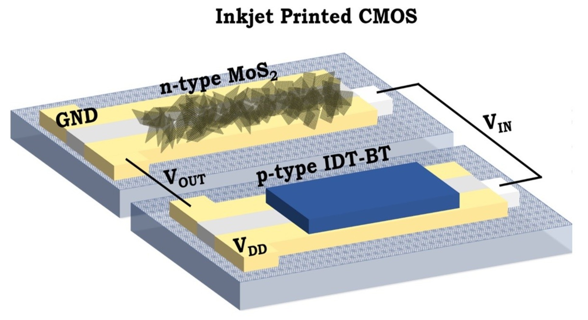
The inks are based on novel two-dimensional (2D) materials, including single-layer molybdenum disulphide (MoS2). These are known as graphene-like materials, because they are made up of sheets that are only a single atom thick, like the atomically thin carbon sheet graphene.
Mass manufacture
Lead researcher Dr Felice Torrisi, from the Department of Chemistry at Imperial, said: “Our new inks represent an important step in creating large-scale printed electronics using novel 2D materials.
“Being able to produce thin, flexible circuits with inkjet printers allows electronics to be printed on a wide range of surfaces, including silicon, plastics, and even textiles. This method also allows for mass production with minimal losses, giving these electronics the scalability to be mass manufactured.”
Researchers have looked into using several materials as printable inks, but to rival classic silicon chips and be useful for wearable devices, inks need to be low-power, low-cost and stable long term. Other inks using organic materials have been produced but are unstable in ambient conditions, such as normal temperatures and moisture levels. This means they degrade in less than 100 hours.
The new 2D-material-based inks can cope with normal temperature and moisture ranges over the long term, making them much more suitable for everyday use as wearable electronics.
Cheap and widely available wearable devices
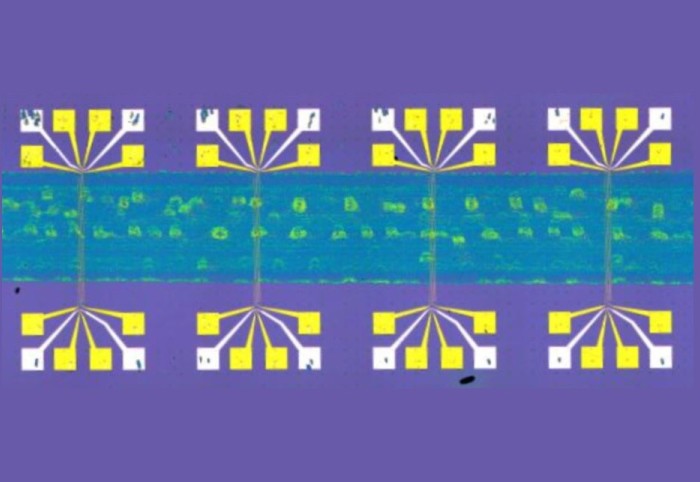
The team have so far shown they can print semiconductors – materials that can both conduct and insulate electric charge, depending on the local properties and conditions of the material. Semiconductors can be tuned to create important components of electrical devices, including transistors and diodes.
The new printed semiconductors are of one type – ‘n-type’ – where electrons are responsible for the current in the electronic devices. The team are now investigating ‘p-type’ printed semiconductors, where the electrons’ counterparts – termed holes – are responsible for the electric current.
Co-author Professor Roman Sordan, from Politecnico di Milano, said: “Our result represents a first step in the integration of inkjet printed n-type 2D transistors and p-type organic transistors into complementary logic gates which are the backbone of modern digital electronics. We hope this brings us closer to cheap and widely available wearable devices.”
-
Below, you can watch Dr Torrisi talk about how applications of 2D materials, such as graphene, can revolutionise industries from healthcare to renewable energy through wearable and malleable materials, for Imperial's Tech Foresight.

-
‘Inkjet printed circuits with two-dimensional semiconductor inks for high-performance electronics’ by Tian Carey et al is published in Advanced Electronic Materials.
Article supporters
Article text (excluding photos or graphics) © Imperial College London.
Photos and graphics subject to third party copyright used with permission or © Imperial College London.
Reporter
Hayley Dunning
Communications Division