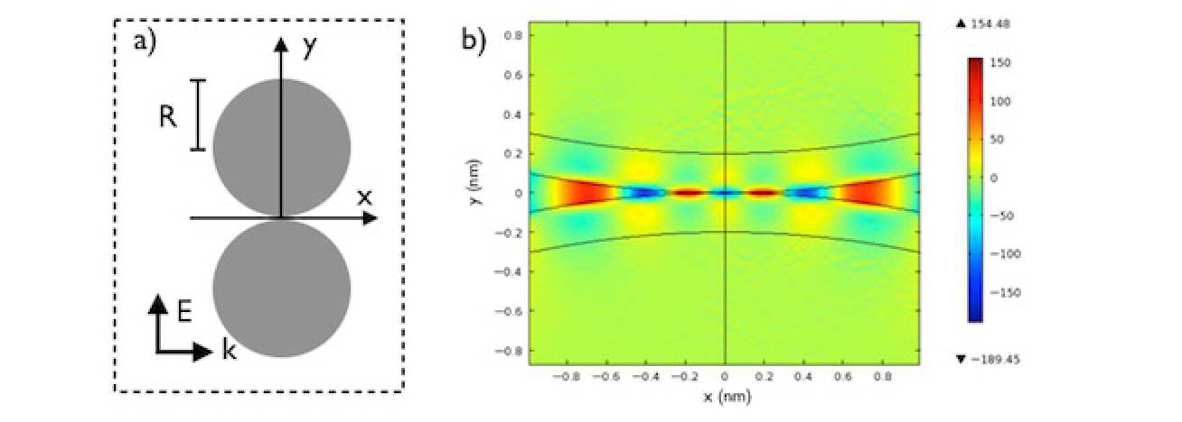
Plasmonic devices are crafted from metallic structures which are shaped on the nanoscale. For example, a pair of kissing silver nanowires of radius ~10 nm (depicted schematically in Figure 1a) can be used for broadband light harvesting in the visible spectrum: the structure collects light from the far field and concentrates its electromagnetic energy near the touching point between the wires.

Close to the touching point the distance between the two nanowire surfaces enters the sub-nanometer regime, where classical electrodynamics solutions fail. A recent study [1], published in the journalPhysical Review Letters, addresses this problem. The paper, which is co-authored by TSM CDT student Aeneas Wiener, develops a new nonlocal electrodynamic solution which extends the validity of classical electrodynamics into the sub-nanometer regime. The authors have successfully applied their scheme to the kissing nanowire geometry, which has lead them to the conclusion that the light harvesting performance of the device is optimised for radii between 50 and 100 nm.
The work has also identified a set of nonlocal optical resonances in this system, contributing to the growing body of knowledge about the physics of nanofocusing device components.
[1] A. I. Fernández-Domínguez, A. Wiener, F. J. García-Vidal, S. A. Maier, and J. B. Pendry. “Transformation-Optics Description of Nonlocal Effects in Plasmonic Nanostructures” Phys. Rev. Lett. 108, 106802 (2012)