Tabs 1
- Room Temperature Probe Station
- Cryo Probe Station
- RF LCR Meter
- Semiconductor Device Analyser
- Vector Network Analyser (VNA)
 Location: Electronics Lab
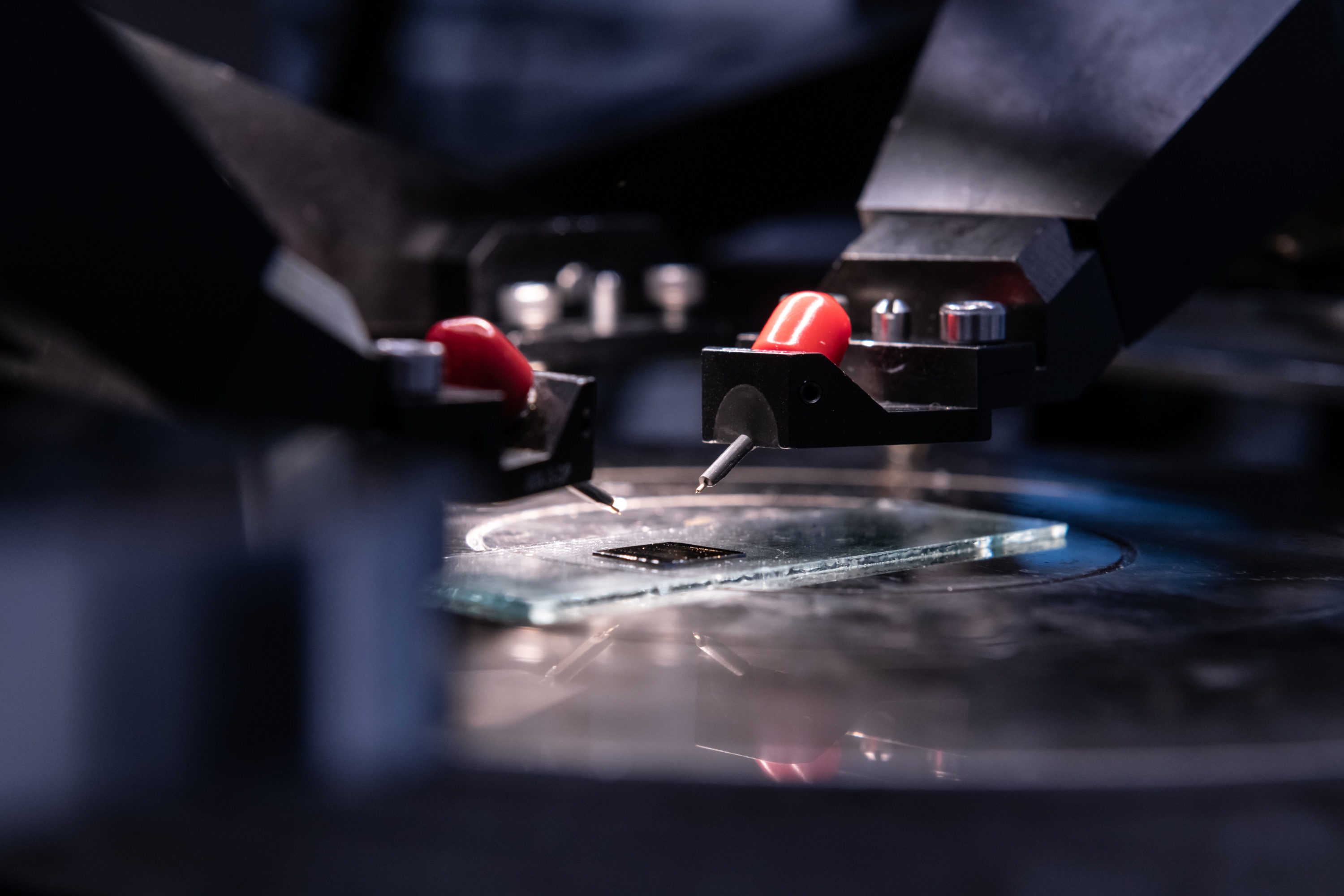
Model: Signatone S-1160
The room-temperature probe station is used to perform electrical measurements on devices at room temperature; ideal equipment for a multi-purpose analytical platform. It can be used to probe small or large geometries by fitting with either high- or low-powered optics. It is also designed to support various precision probing applications, including MCMs, hybrids and wafers. It is also compatible with magnetic and vacuum base micro-positioners. In addition, it has a purpose-built heating stage that allows measurement at temperatures up to 250°C with 0.1°C accuracies.
 Location: Electronics Lab
Model: Janis Microwave (MW) Cryo Probe Station
The Microwave (MW) Cryo-probe Station is designed to provide affordable vacuum and cryogenic probing of wafers and devices. The on-wafer measurements could be performed under external electrical bias, and magnetic field (up to 0.15 T) applied in horizontal or vertical directions, in wide temperature (10 K – 600 K) and frequency (d.c. – 65 GHz) ranges. The system can be used in various fields, including superconductivity, MEMS, ferroelectrics, nanoscale electronics, material sciences, and optics.
RF LCR Meter (inductance, capacitance and resistance)
Location: Electronics Lab
Model: Agilent 4287A RF LCR Meter
The 4287A RF LCR Meter offers accurate, reliable and fast measurements from 1 MHz to 3 GHz to improve the quality and throughput of electronic component testing in production lines. The 4287A employs the direct-current voltage-measurement technique instead of the reflection-measurement technique, which yields accurate measurements over a wide impedance range.
 Location: Electronics Lab
Model: Keysight B1500A
The Semiconductor Device Analyser provides a wide range of measurement capabilities to cover the electrical characterisation and evaluation of devices, materials, semiconductors, active/passive components, or virtually any other electronic device with uncompromised measurement reliability and efficiency.
It provides a wide range of measurement capabilities to cover the electrical characterisation and evaluation of devices, materials, semiconductors, active/passive components, or virtually any other electronic device with uncompromised measurement reliability and efficiency.
Location: Electronics Lab
Model: Keysight P5008A Vector Network Analyser 100 kHz - 53 GHz
50 MHz - 40 GHz, S-Parameter Vector Network Analyzer.
This is a flexible, high-performance, compact VNA that provides a frequency range of 100 kHz to 53 GHz. It allows a wide range of measurement applications to gain deeper insight into your RF test. It features the same intuitive GUI as Keysight’s high-performance PNAs.
Tabs 2
 Location: Electronics Lab
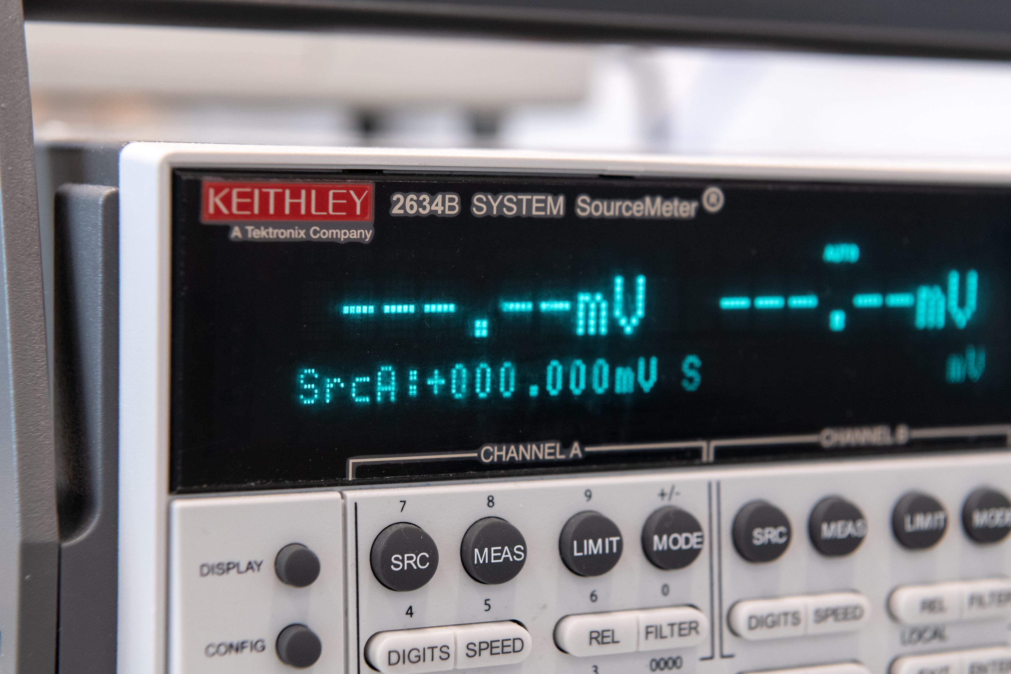
Model: Keithley Source Meter 2634B
Keithley’s Series 2600B System SMU instruments are the industry standard current-voltage source and measure solution for highly automated production test applications. Both dual- and single-channel models tightly integrate a precision power supply, accurate current source, DMM, and electronic load with a pulse generating capabilities. Plus, TSP® technology runs complete test programs for automated system applications, and TSP-Link® technology enables daisy-chaining up to 64 channels for high-volume parallel tests.
 Location: Laser Lab
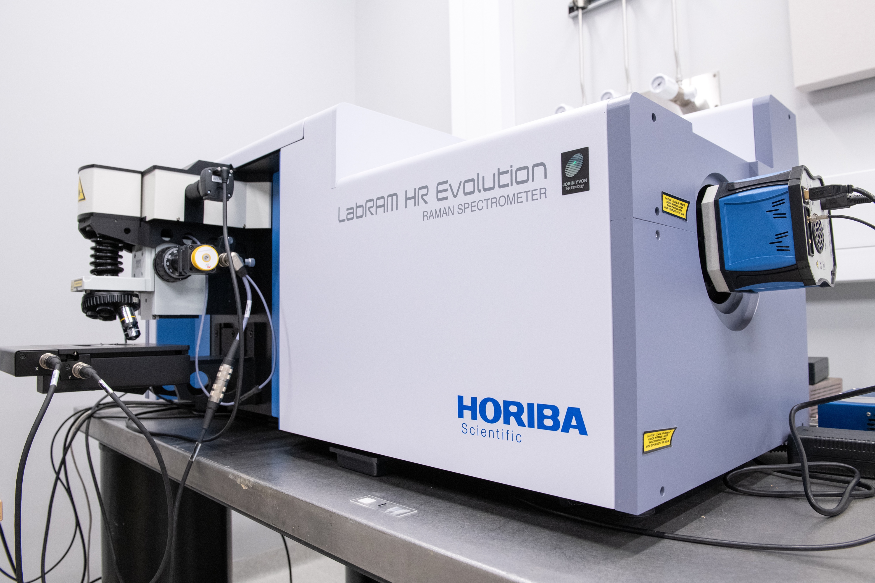
Model: Horibva Labram HR Evo
The LabRAM HR Evolution Raman microscopes are ideally suited for micro and macro measurements and offer advanced confocal imaging capabilities in 2D and 3D. The actual confocal Raman microscope enables the most detailed images and analyses to be obtained quickly and confidently.
With guaranteed high performance and intuitive simplicity, the LabRAM HR Evolution is the ultimate instrument for Raman spectroscopy. They are widely used for standard Raman analysis, PhotoLuminescence (PL), Tip Enhanced Raman Spectroscopy (TERS) and other hybrid methods.
 Location: Laser Lab
Model: Oxford Instrument Asylum - MFP-3D
The MFP-3D Origin™ offers high-resolution imaging, supports large samples, most imaging modes, and many accessories.
 Location: Characterisation Lab
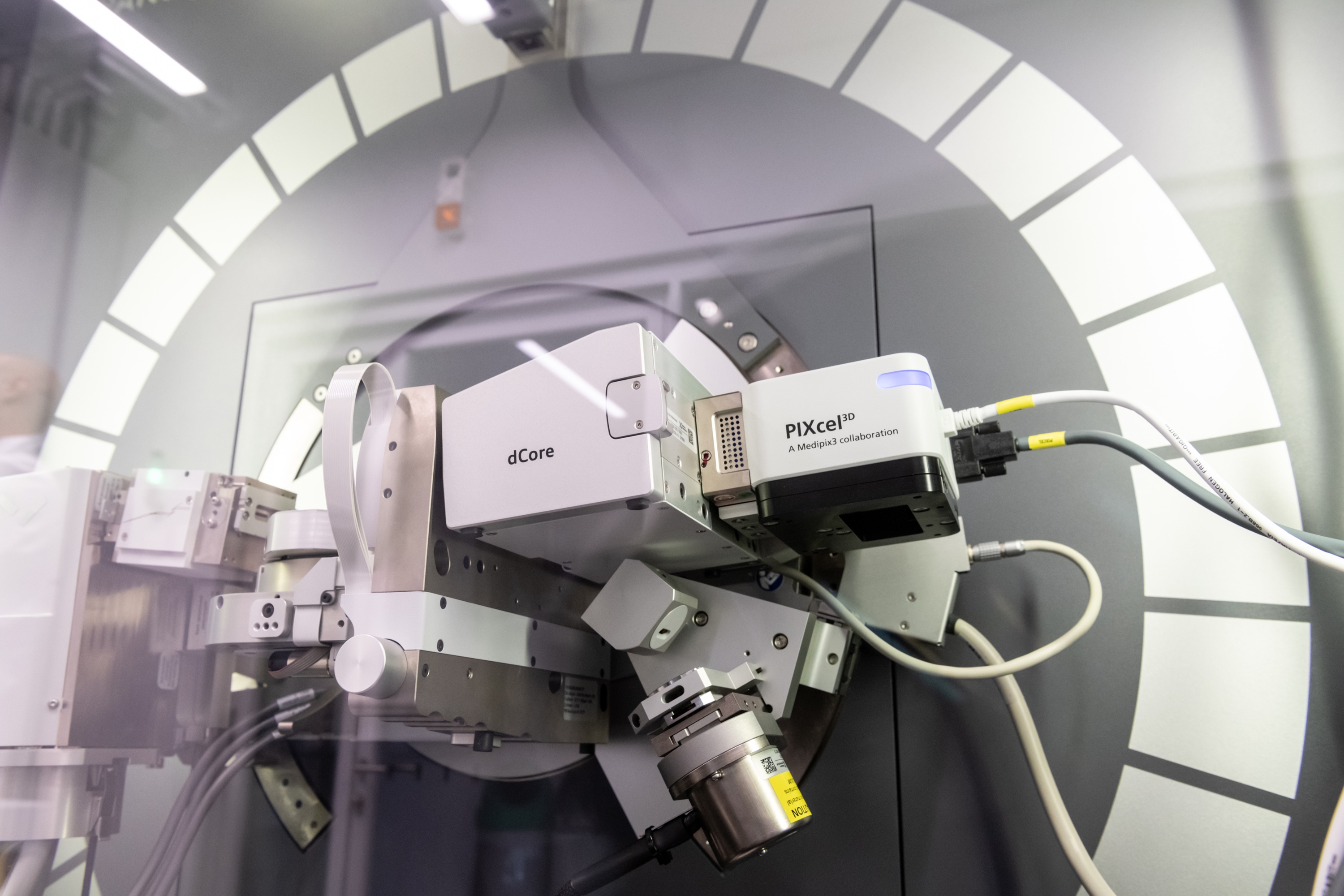
Model: Malvern Analytical Empyrean MultiCore High-Performance X-ray Diffractometer
Empyrean covers the most extensive X-ray diffraction, scattering and imaging applications in one instrument. The MultiCore Optics enable the widest variety of measurements without any manual intervention. Empyrean can measure all sample types - from powders to thin films, from nanomaterials to solid objects - on a single instrument.
Moreover, Empyrean not only meets the high expectations of scientists and XRD experts today but will continue to do so as research themes evolve. Empyrean is ideal for teaching purposes, thanks to the large doors that open entirely, allowing access to the system to several people, but at the same time is perfect for performing measurements in demanding R&D environments in several industries.
Tabs 3
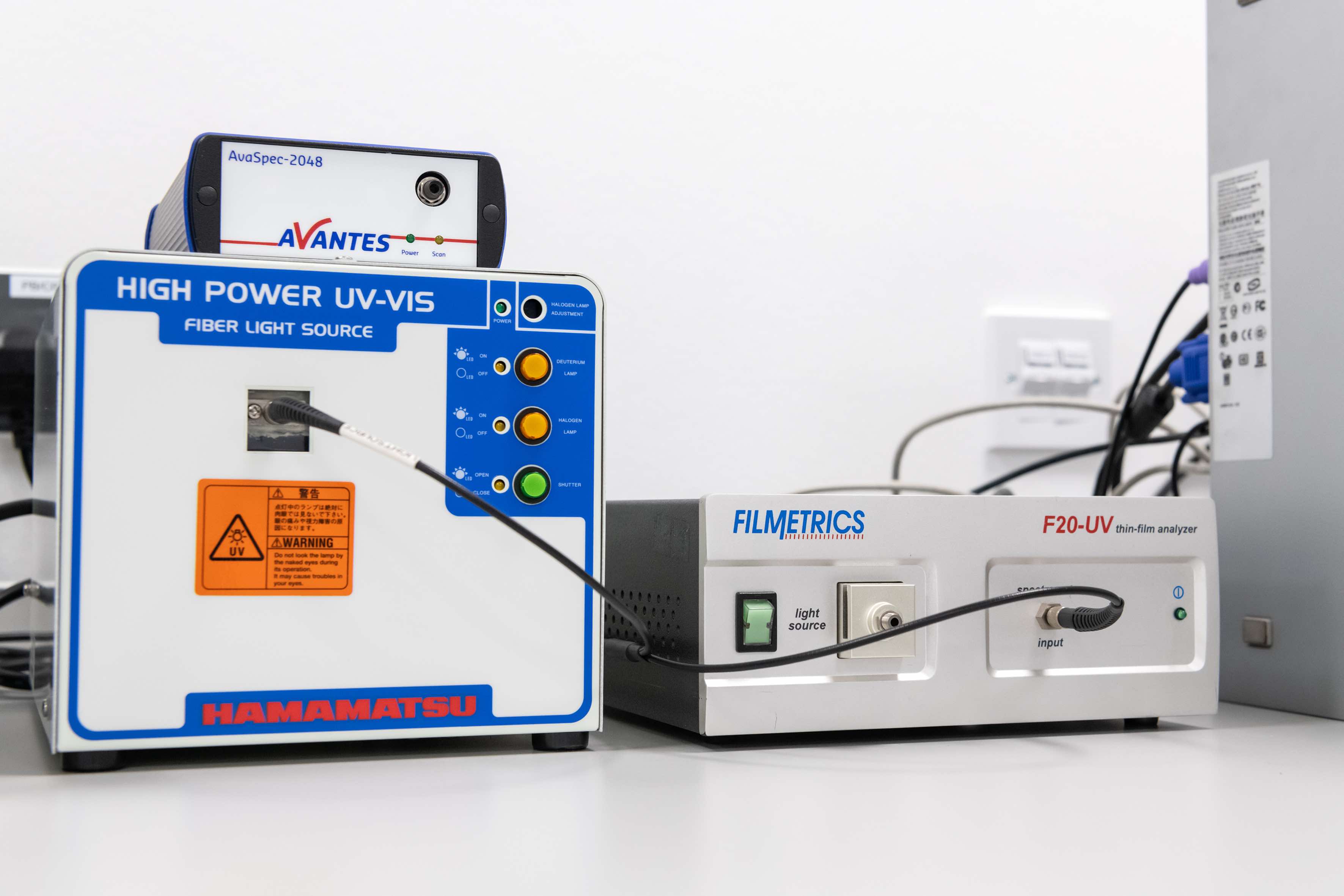 Location: Clean Room
Model: Filmetric F20-UV
The F20–UV is a thin film analyser that can measure thickness and refractive index in less than a second. Like all thickness measurement instruments, it connects to the computer's USB port and is set up in minutes. The thickness measurement ranges between 1 nm – 40 μm, with a wavelength range between 190 – 1100 nm.
Features included in the F20–UV include an integrated spectrometer, a flattening filter for highly reflective substrates, a FILmeasure standalone software for remote data analysis, reflectance standards, thickness standards, an SS-3 sample stage with fibre optic cable and a TH1-lamp.
ZEISS LSM 800 MAT Confocal Microscope System with Axio Image
Location: Molecular Sciences Research Hub
Model: 3D Laser Scanning Confocal Microscope
ZEISS LSM 800 enables precise, three-dimensional imaging of microstructures and surfaces.
Combining confocal fluorescence and other contrasting techniques in one instrument allows a high-precision examination of nanomaterials, metals, polymers, and semiconductors with maximum information content.
The system accurately captures 3D topography and investigates nanometre-scaled structures without causing surface damage.
 Location: Deposition Lab
Model: KLA Tencor D-600 Profiler
The KLA Alpha-Step D-600 stylus profiler is capable of measuring 2D and 3D thin and thick film step heights from a few nanometres to 1200µm. The D-600 also supports 2D and 3D measurements of roughness, plus 2D bow and stress for R&D and production environments. The D-600 includes a motorized stage with a 200mm sample chuck and advanced optics with enhanced video controls.
Location: Clean room
Model: KLA Tencor D-500 Profiler
The Alpha-Step D-500 stylus profiler is capable of 2D step height measurement from a few nanometers up to 1200µm. The D-500 also supports 2D measurements of roughness, bow and stress for R&D and production environments. The D-500 stylus profilometer includes a manual 140mm stage and advanced optics with enhanced video controls.
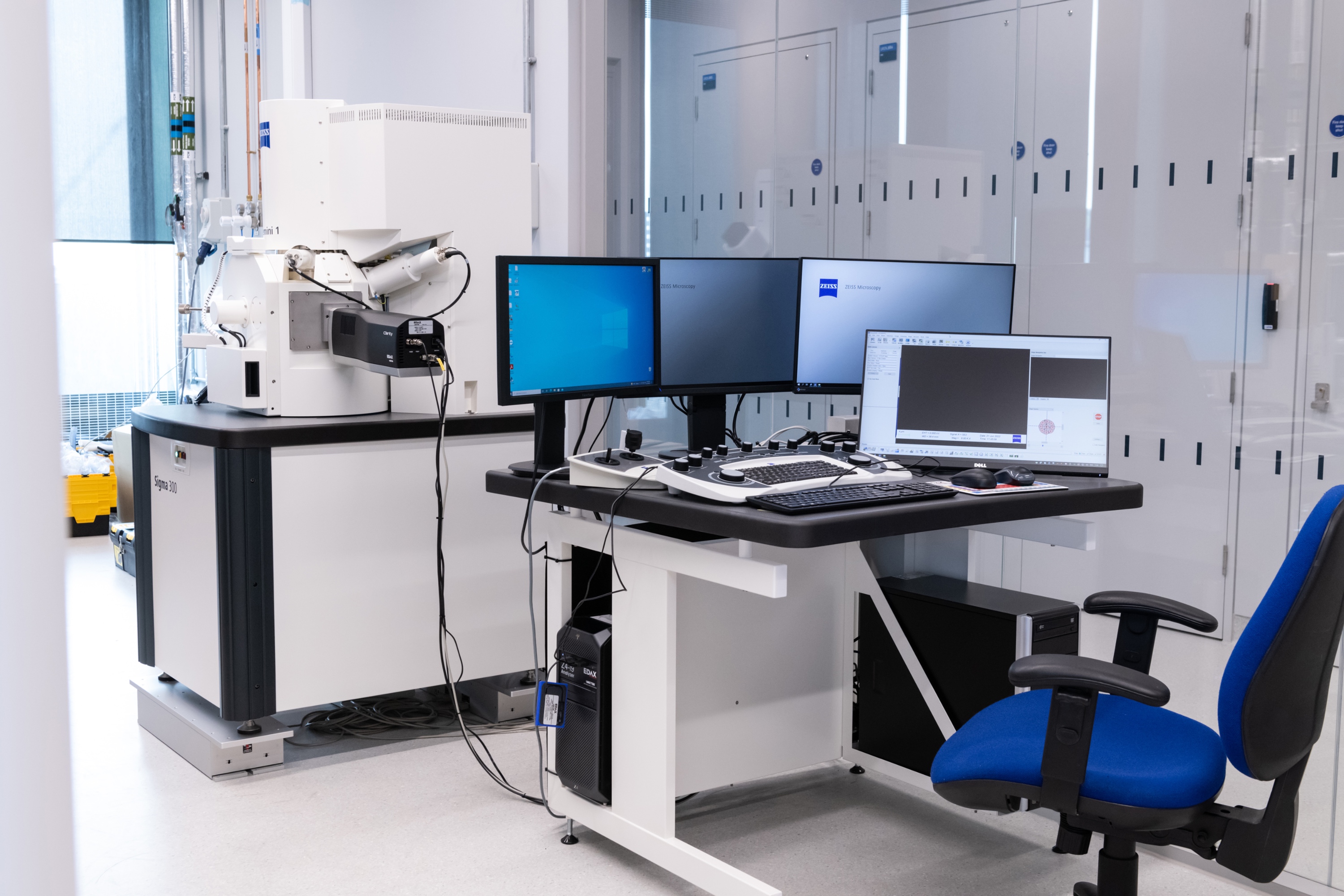 Location: Characterisation Lab
Model: Gemini 1 Zeiss Sigma 300 w/ Clarity EBSD
Combine field emission SEM (FE-SEM) technology with analytics. Profit from proven Gemini electron optics. Choose from a variety of detector options: image particles, surfaces, and nanostructures in materials science investigate semiconductor or medical devices, and geological or biological samples.
Save time with the semi-automated 4-step workflow of Sigma: structure your imaging and analysis routines and increase productivity. FE-SEM users of all disciplines in research and industry labs now benefit from a resolution of 1.3 nm at 1 kV in ZEISS Sigma 500 and better usability.
How to access
To access our facilities, please email royce@imperial.ac.uk.
.jpg)