Tab 1
- Magnetron Sputtering HEX-L
- Magnetron Sputtering HEX
- Metal PVD and Graphene CVD
- Reactive Ion Etching
- Dicing Saw
- Surface Profiler
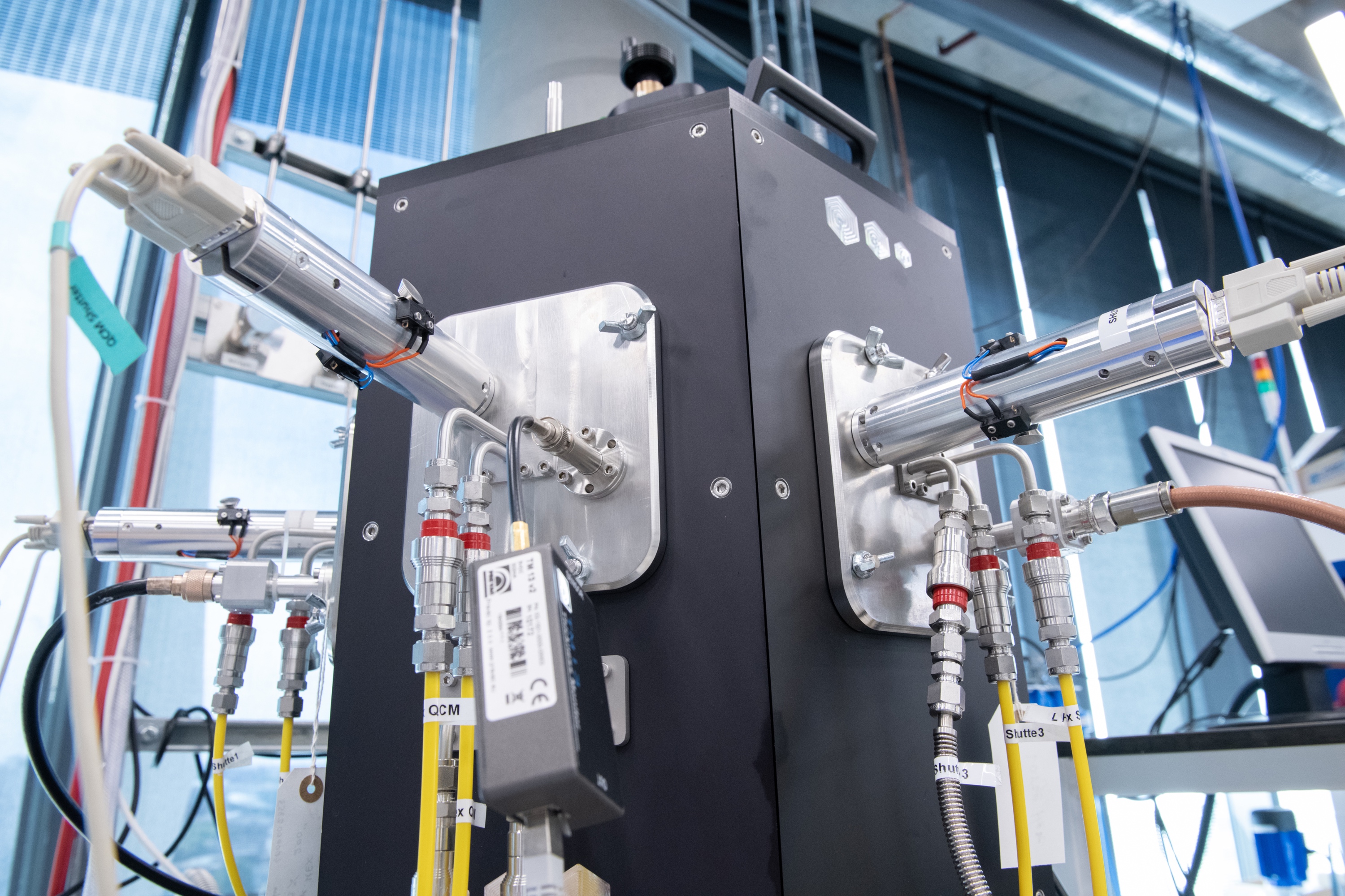 The Korvus Technology HEX deposition system provides an economical solution for Physical Vapour Deposition (PVD), suitable for teaching and research. Its modular construction allows various vital elements to be exposed, discussed and interacted with, enabling student laboratories to fully explore the mechanical, material and growth elements of thin film research and nano-materials. Our system benefits from a rotatable 4” sample holder with heating capabilities up to 800 oC, and one 2” RF and two 2” DC magnetron, allowing multilayer and/or co-sputtered thin film deposition.
The HEX-L system is allocated for nitride and oxide thin film deposition.
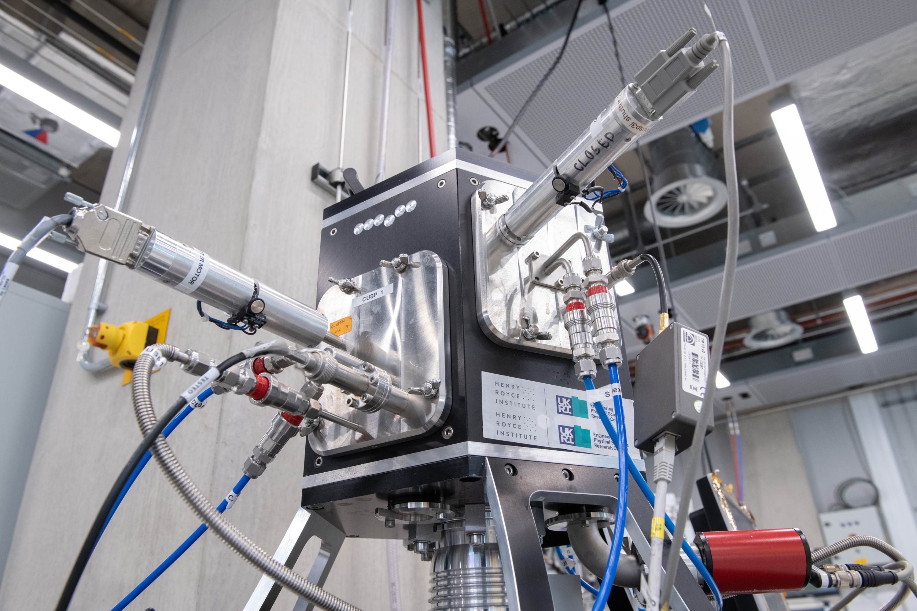 The Korvus Technology HEX deposition system provides an economical solution for Physical Vapour Deposition (PVD), suitable for teaching and research. Its modular construction allows various vital elements to be exposed, discussed and interacted with, enabling student laboratories to fully explore the mechanical, materials and growth elements of thin film research and nano-materials. Our system benefits from a rotatable 4” sample holder with two 2” DC sputtering sources, allowing bi-layer thin film deposition.
The HEX system is allocated for metal deposition.
 This is a combined system that consists of a Physical Vapour Deposition (PVD) (thermal evaporation) chamber, which is used for the deposition of copper thin films, and a vertical Chemical Vapour Deposition (CVD) system used for graphene deposition. Both chambers are connected with a common load-lock that allows the deposition of high-quality graphene on 4” Si wafers. A copper thin film is deposited on a 4” wafer, which is then transferred (without breaking the vacuum) to the CVD reactor for consequent graphene growth. The CVD reactor also benefits from an RF plasma source to pre-crack the reacting gas molecules.
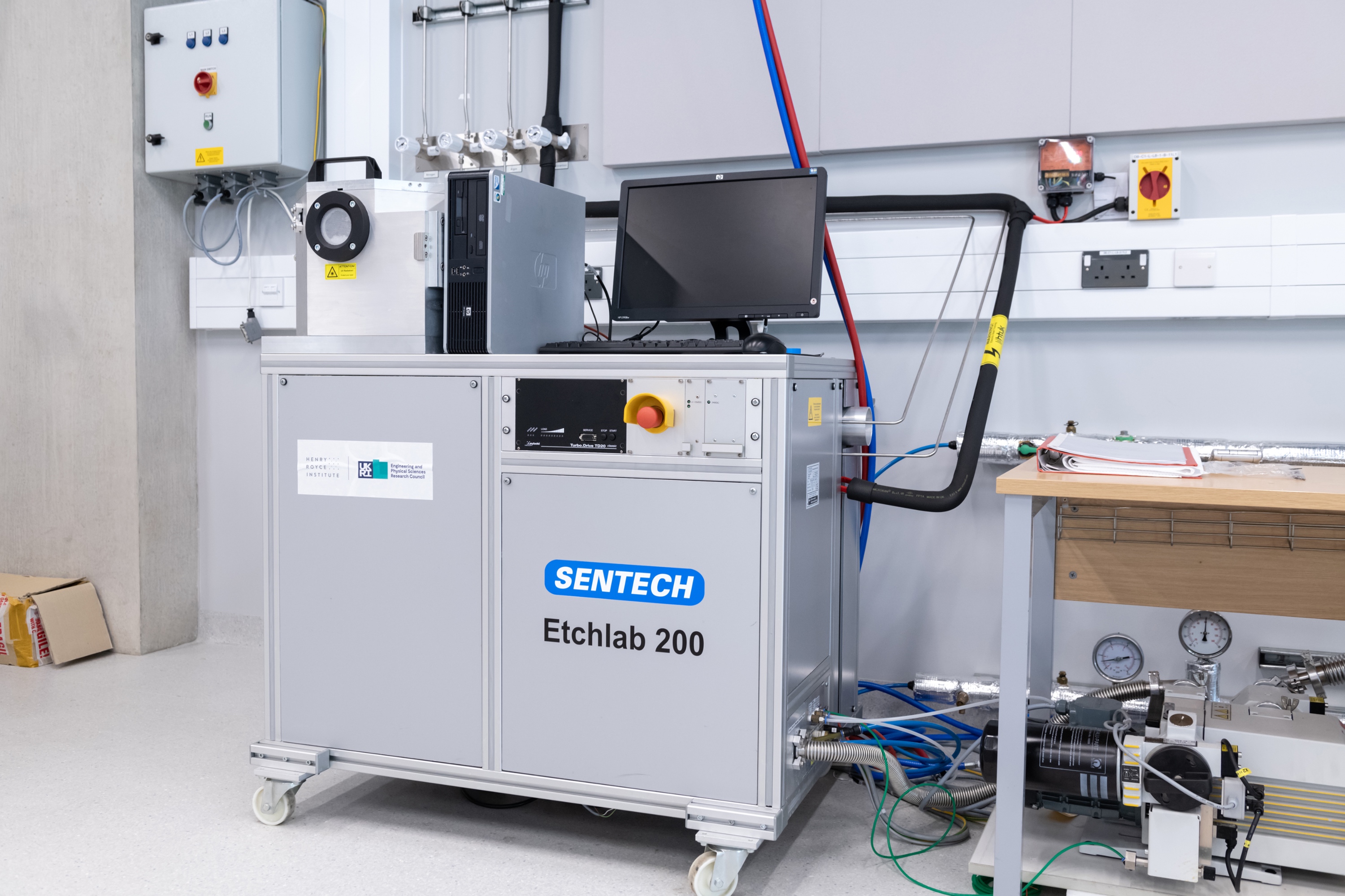 Reactive Ion Etching (RIE) is a process whereby chemical etching is accomplished through the bombardment of ions. This technique can be used for etching various materials for top-down fabrication of multi-layer thin films or functional devices such as metals, semiconductors, dielectric materials or combinations. It also has the advantage of using multiple gases such as C4F8, Argon, Oxygen and Nitrogen.
 The MicroAce 66 is a 6” automatic dicing saw configured with a 2.4kW spindle. It could be used for various applications including cutting demanding and thick wafers with micron precision.
It offers a high level of configurability to get the best performance out of your application.
 The KLA Alpha-Step D-600 stylus profiler is capable of measuring 2D and 3D thin and thick film step heights from a few nanometres to 1200µm. The D-600 also supports 2D and 3D measurements of roughness, plus 2D bow and stress for R&D and production environments. The D-600 includes a motorized stage with a 200mm sample chuck and advanced optics with enhanced video controls.
How to access
To access our facilities, please email royce@imperial.ac.uk.
.jpg)