Tabs 1
- Karl Suss Mask Aligner
- OAI Mask Aligner
- Spin Coater
- Wide Beam Ion Milling
- ICP - RIE
- Reactive Ion Etching
 Location: Clean Room Yellow Room Photolithography Suite
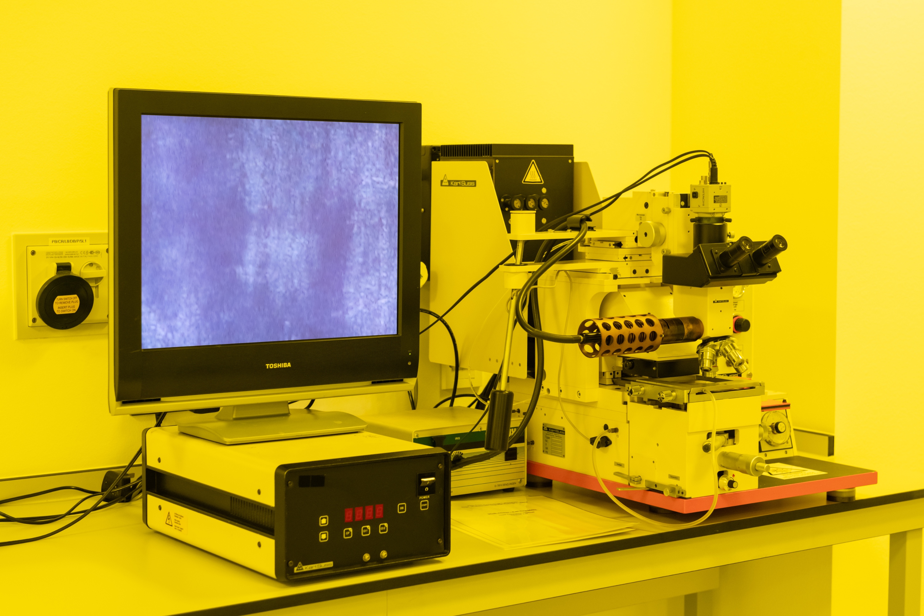
Model: Karl Suss Mask Aligner MJB3
Easy to use and compact in size, the SUSS MicroTec MJB3 represents the perfect system for laboratories and small-volume production. As an inexpensive photolithography solution, the MJB3 has set industry standards specifically for processing small substrates and pieces up to 100 mm. Equipped with a reliable, high-precision mask alignment and high-resolution printing capability in the submicron range, the MJB3 is unsurpassed by any comparable machine.
 Location: Clean Room Yellow Room Photolithography Suite
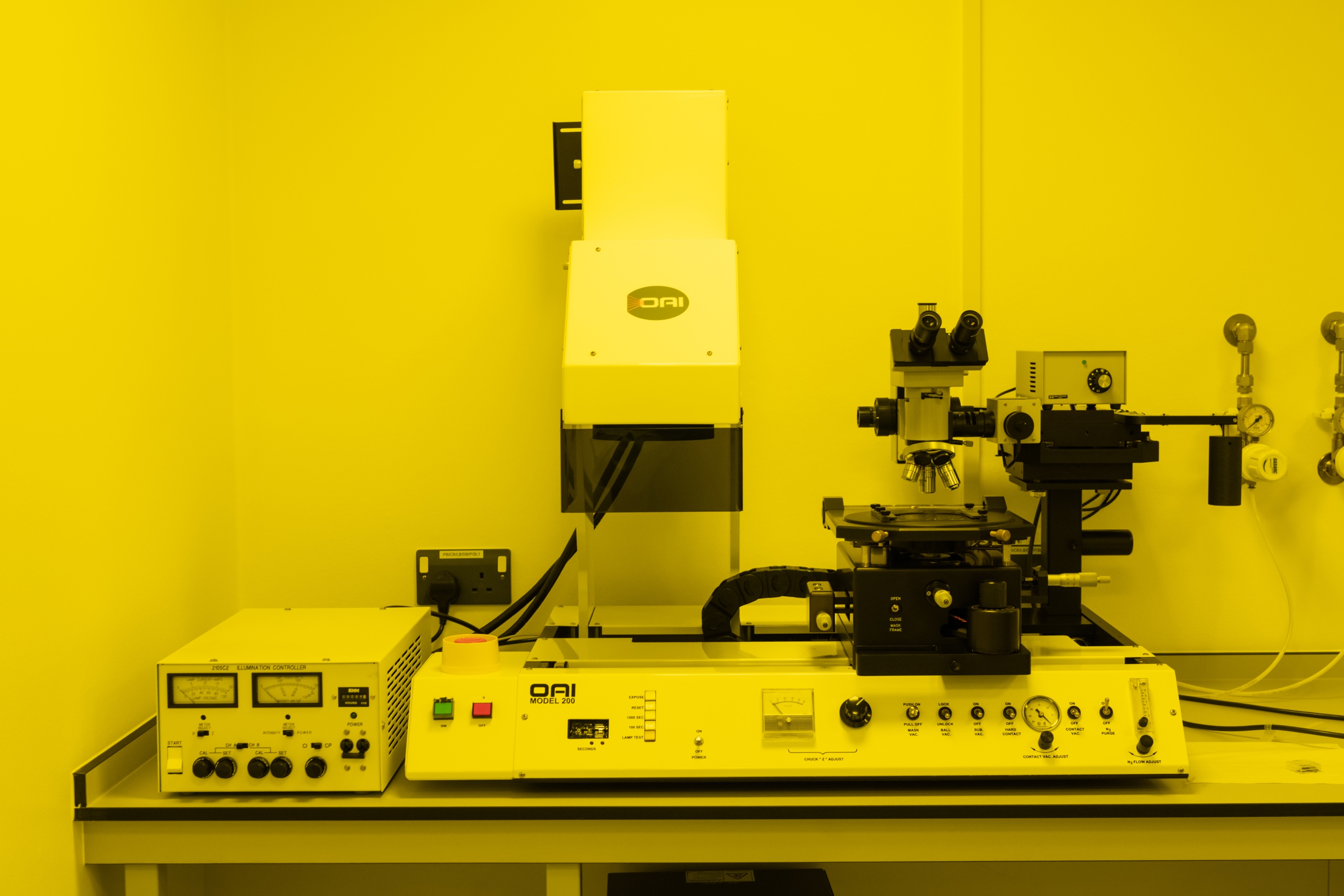
Model: OAI MODEL 204
The Model 200 is a tabletop mask Aligner that requires minimal cleanroom space. It offers an economical alternative for R&D, or limited scale, pilot production. Utilising an innovative, air-bearing/vacuum chuck levelling system, the substrate is levelled quickly and gently for parallel photo mask alignment and uniform contact across the wafer during contact exposure. The system is capable of one-micron resolution and alignment precision.
The alignment module features mask insert sets and quick-change wafer chucks that facilitate using various substrates and masks without requiring special tools for reconfiguration. The alignment module incorporates micrometres for the X, Y, and Z-axis. The Model 200 Mask Aligner features a dependable OAI UV Light Source, which provides collimated UV light in Near or Deep UV using lamps ranging in power from 200 to 2000 watts.
Dual-sensor optical feedback loops are linked to the constant intensity controller to provide control of exposure intensity within ±2% of the desired intensity. This Mask Aligner is a flexible, economical solution for any entry-level mask alignment and UV exposure application and is also available with a LED Light Source.
Location: Clean Room Yellow Room Photolithography Suite
Model: Suss MicroTec Delta+6RC
SUSS MicroTec‘s LabSpin platform represents the next generation of manual spin coater and developer systems that have been developed specifically for laboratory and R&D. Designed for various photolithography chemicals, LabSpin systems provide uniform, precise and repeatable spin coating results on the wafer through its advanced process chamber design. The LabSpin is available in various versions, such as a tabletop and built-in unit. Built-in platforms are designed for integration into a wet bench and a glove box or are used in the SUSS LabCluster. LabSpin6 is suitable for round substrates up to 150 mm in diameter or square substrates up to 100x100 mm. LabSpin8 is suitable for round substrates up to 200 mm in diameter or square substrates up to 150x150 mm. With a wide range of substrate holders, even fragments and unique shapes can be processed without problems. The LabSpin platform is characterised by a compact, space-saving design and requires little clean room space.
The large variety of LabSpin options allows a very wide range of applications. Coatings can be applied manually with syringes, semi-automatically with cartridges or with up to two fully automatic dispensing systems. In addition to edge coating, edge bead removal and puddle development, further options are available.
 Location: Clean Room
Model: scia Mill 150
The scia Mill 150 is designed for highly uniform ion beam etching of single substrates up to 150 mm. The system is equipped with a circular broad beam ion source with a diameter of 218 mm. The source operates with inert gases (Ion Beam Etching) as well as with reactive gases (Reactive or Chemically Assisted Ion Beam Etching). The substrates will be mounted on a tiltable and rotatable substrate holder, which enables helium backside thermal contact for effective substrate cooling.
For faster processing and with stable process conditions a load lock system is installed, and samples of up to 150 mm in diameter are transferred automatically via the load lock into the process chamber.
A typical application is the nano- and micro structuring of complex multilayers of metallic and dielectric materials. An optical endpoint detection system is also integrated for the recognition of etched species and to apply a defined etch stop.
 Inductively Coupled Plasma - (ICP-RIE)
Location: Clean Room
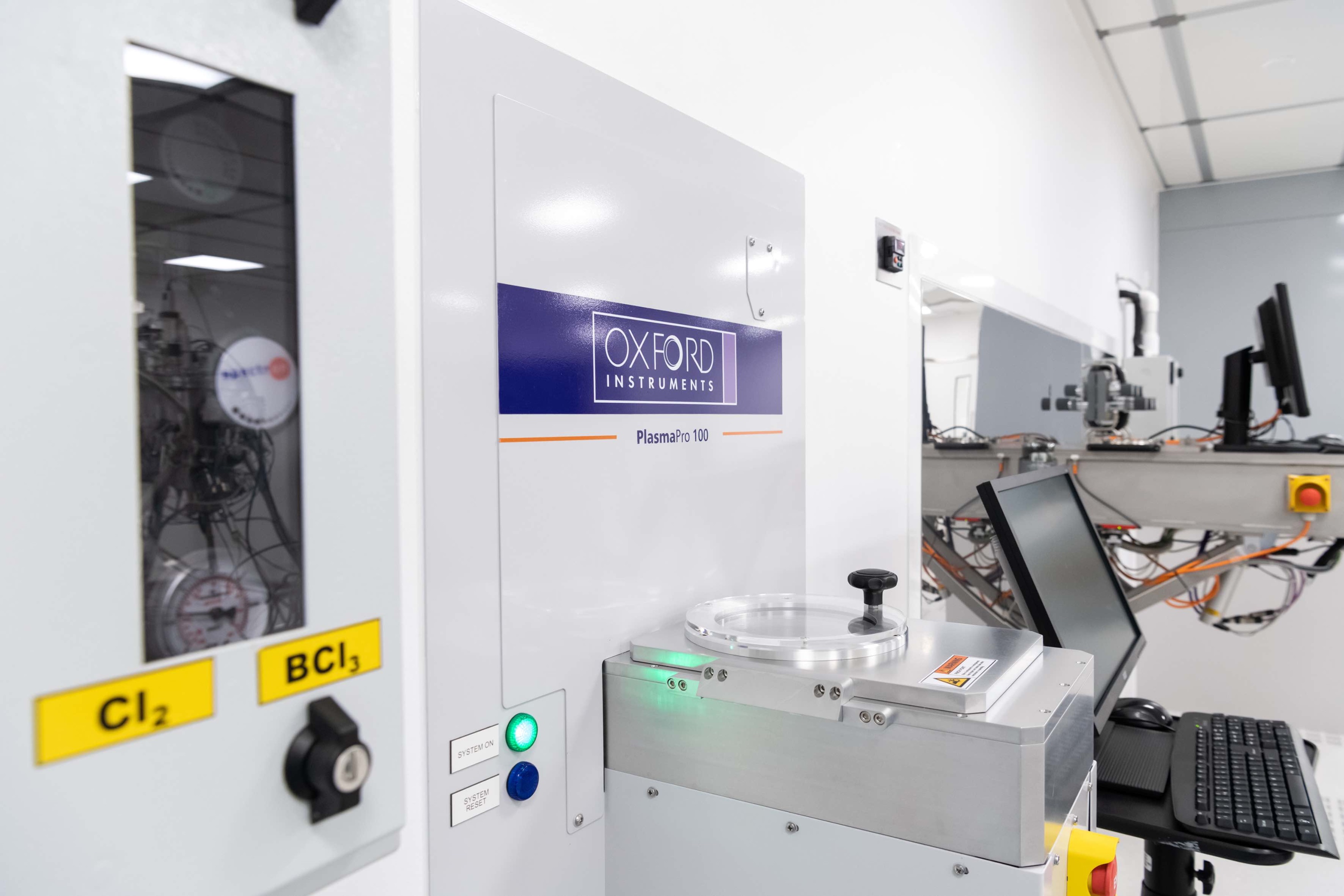
Model: PlasmaPro 100 Cobra ICP Etch
The PlasmaPro 100 Cobra ICP RIE system utilises a high-density inductively coupled plasma to achieve fast etch rates. The process modules offer excellent uniformity, high-throughput, high-precision, and low-damage processes for wafer sizes up to 200mm, supporting several markets, including laser optoelectronics, power electronics, RF and MEMS, and sensors.
 Location: Deposition Lab
Reactive Ion Etching (RIE) is a process whereby chemical etching is accomplished through the bombardment of ions. This technique can be used for etching various materials for top-down fabrication of multi-layer thin films or functional devices such as metals, semiconductors, dielectric materials or combinations. It also has the advantage of using multiple gases such as C4F8, Argon, Oxygen and Nitrogen.
Tabs 2
 Location: Characterisation Lab
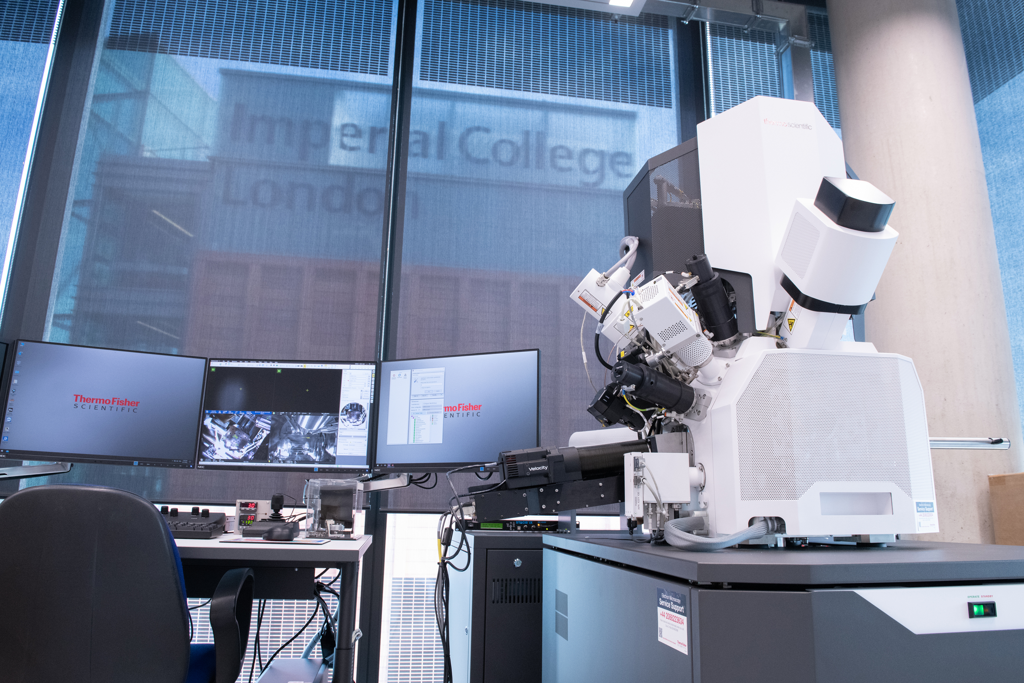
Model: Thermo Scientific Scios - 2 HiVac with Retractable RGB CL Detector w/ Velocity EDSB
Backscattered electron and secondary electron imaging
The innovative NICol electron column provides the foundation of the system’s high-resolution imaging and detection capabilities. It offers excellent nanoscale details, with a wide range of working conditions, whether operating at 30 keV in STEM mode (to access structural information) or at lower energies (to obtain charge-free, detailed surface information). With its unique in-lens Thermo Scientific Trinity Detection System, the Scios 2 DualBeam is designed to simultaneously acquire angular and energy-selective secondary electron (SE) and BSE imaging.
Fast access to detailed nanoscale information is possible not only top-down but also on tilted specimens or cross-sections. Optional below-the-lens detectors and an electron-beam-deceleration mode ensure quick and easy simultaneous collection of all signals, revealing the minor features in a material surface or cross-section. Fast, accurate, and reproducible results are obtained thanks to the unique NICol column design with full auto alignments.
Location: Clean Room - E-Beam Lithography Suite
Model: E- Beam Writer Raith e-LINE 30 keV/Agilent 4287A
The Combined Magnetron Sputtering and Electron Beam Deposition System is an ultra-high vacuum sputtering and evaporation system.
The e_line uses a focused electron beam to expose a thin layer of electron beam resist changing the solubility of the resist in its developer. For positive resist submerging in, the developer will remove the exposed resit. For negative resist, the unexposed resist will be removed. These structures can be samples themselves or be used as stencils for the deposition of thin film materials.
It consists of three sources for DC and RF magnetron sputtering and a four-pocket e-beam evaporator. It has two types of substrate holders: one is with an active cooling system, while the second is with a heating stage to 800°C and an RF biasing option. Both substrate holders can handle wafers up to 4” in diameter. -5-30 kV beam energies,100um write field size, >2nm stitching error, 7.5-120um beam appatures, common to achieve 20nm feature size with 10nm gaps, 3D SEM stage for angled sample inspection, >5nm SEM resolution.
How to access
To access our facilities, please email royce@imperial.ac.uk.
.jpg)