Tabs 1
- Pulsed Laser Deposition
- Magnetron Sputtering HEX-L
- Magnetron Sputtering HEX
- Metal PVD and Graphene CVD
- Magnetron Sputtering
- E-Beam Deposition System
 Location: Laser lab
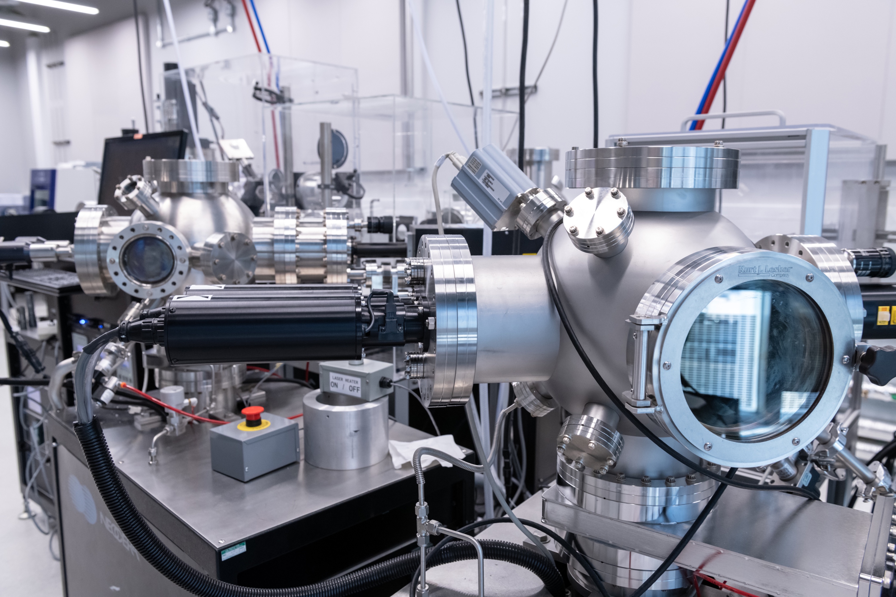
Model: Neocera Pulsed Laser Deposition System
Pulsed Laser Deposition (PLD) is a physical vapour deposition technique used to produce thin films of complex materials over various background gas compositions or pressures. Our PLD system consists of four fully-automated deposition chambers, each equipped with a six-position target carrousel that allows the deposition of multilayer structures of up to six different materials.
There are two deposition chambers with a diode substrate heater that allows deposition at temperatures up to 1200°C. Layer-by-layer growth of functional materials, controlled by a kSA 400 RHEED system, is also available in our specialised UHV deposition chamber.
 Location: Deposition Lab
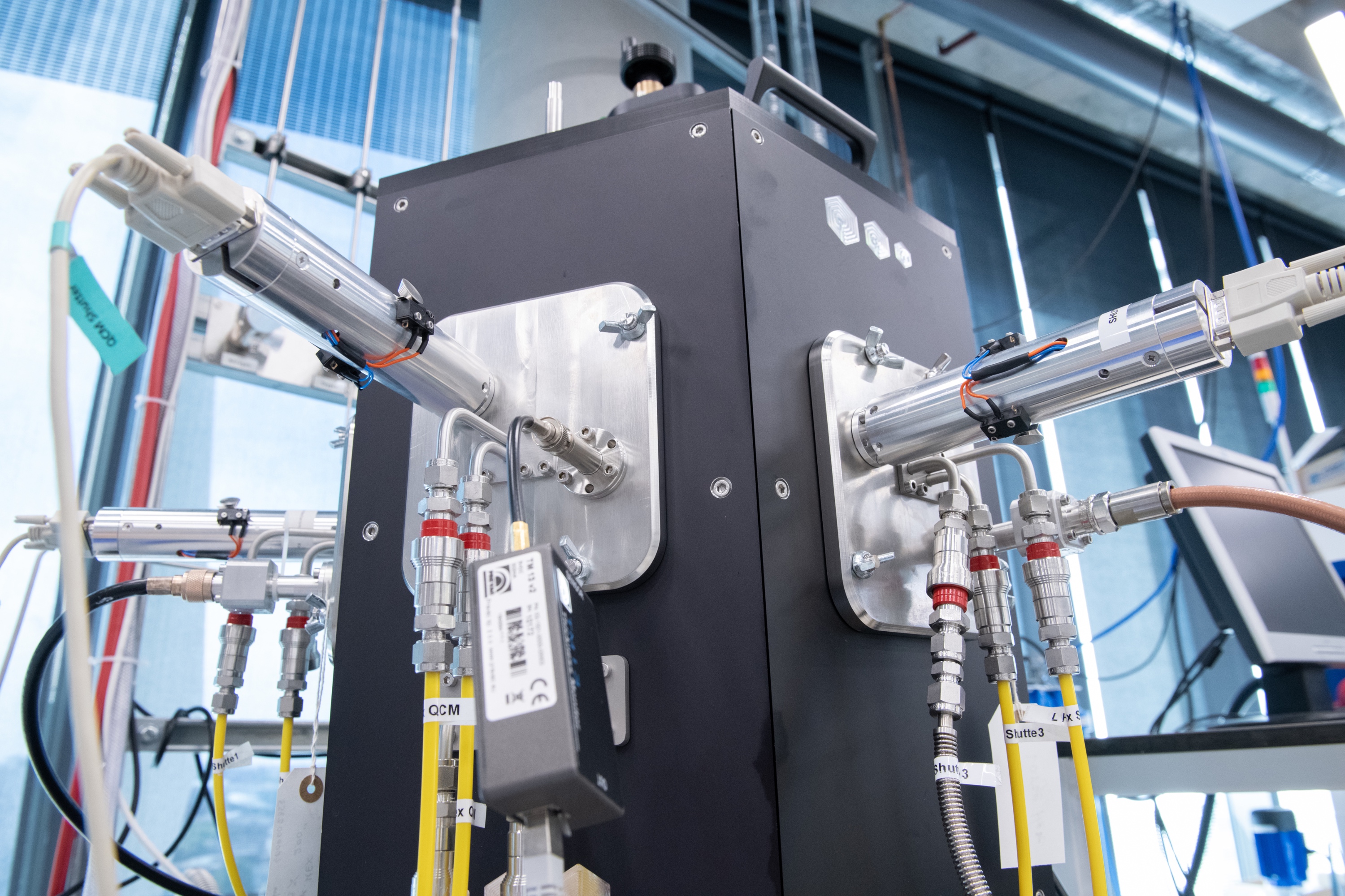
Model: KORVIS - Hex L
The Korvus Technology HEX deposition system provides an economical solution for Physical Vapour Deposition (PVD), suitable for teaching and research. Its modular construction allows various vital elements to be exposed, discussed and interacted with, enabling student laboratories to fully explore the mechanical, material and growth elements of thin film research and nano-materials.
Our system benefits from a rotatable 4” sample holder with heating capabilities up to 800 oC, and one 2” RF and two 2” DC magnetron, allowing multilayer and/or co-sputtered thin film deposition.
The HEX-L system is allocated for nitride and oxide thin film deposition.
 Location: Deposition Lab
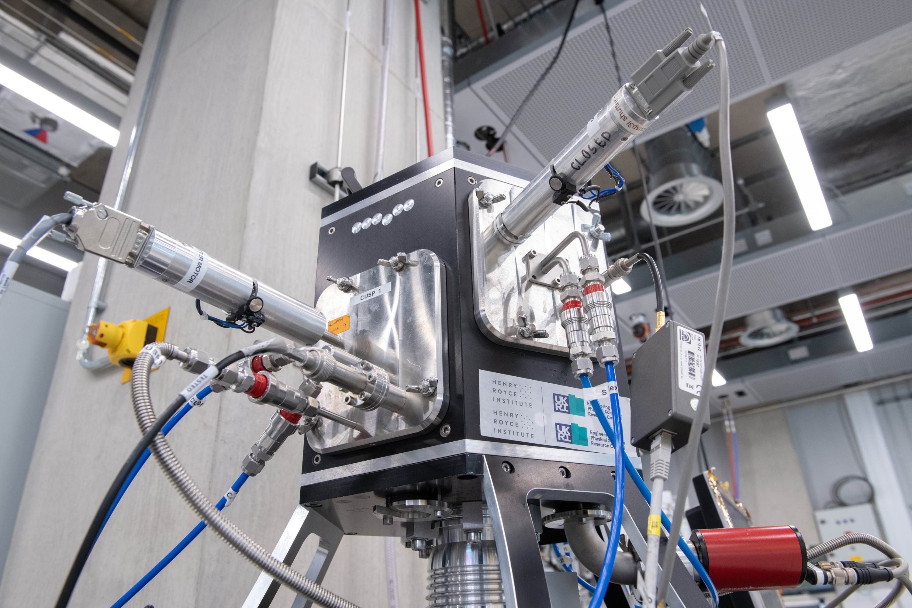
Model: KORVIS - HEX
The Korvus Technology HEX deposition system provides an economical solution for Physical Vapour Deposition (PVD), suitable for teaching and research. Its modular construction allows various vital elements to be exposed, discussed and interacted with, enabling student laboratories to fully explore the mechanical, materials and growth elements of thin film research and nano-materials. Our system benefits from a rotatable 4” sample holder with two 2” DC sputtering sources, allowing bi-layer thin film deposition.
The HEX system is allocated for metal deposition.
 Location: Deposition Lab
Model: VG Scienta Nanoedge 100
This is a combined system that consists of a Physical Vapour Deposition (PVD) (thermal evaporation) chamber, which is used for the deposition of copper thin films, and a vertical Chemical Vapour Deposition (CVD) system used for graphene deposition. Both chambers are connected with a common load-lock that allows the deposition of high-quality graphene on 4” Si wafers.
A copper thin film is deposited on a 4” wafer, which is then transferred (without breaking the vacuum) to the CVD reactor for consequent graphene growth. The CVD reactor also benefits from an RF plasma source to pre-crack the reacting gas molecules.
 Location: Clean Room
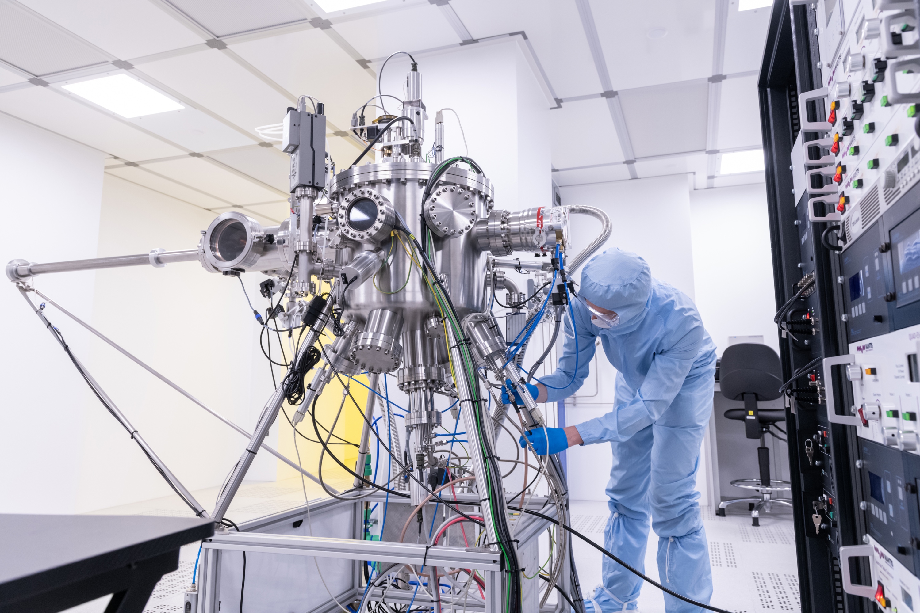
Magnetron Sputtering (HIPIMS)
The Magnetron Sputtering System is an ultra-high vacuum deposition system.
It consists of three sources for DC and RF magnetron sputtering. It has a 4” in diameter rotating substrate holder with a heating stage to 800°C and RF biasing option. The system has High-Power Impulse Magnetron Sputtering (HiPIMS) deposition capability.
It is equipped with two Ionautics’ HiPSTER 1 power supplies with Reactive Sputtering control and a HiPSTER synchronisation unit that allows the user to control the pulsing of both HiPSTER HiPIMS power supplies.
 Location: Clean room
The E-beam evaporation system is an ultra-high vacuum deposition system.
It consists of an MBE-Komponenten Multi Pocket Electron Beam Evaporator with 4 pockets, a hearth capacity 8 cm³ each, and a maximum power of 5kW. It has a 4” in diameter rotating substrate holder with a heating stage of 800°C and QCM to monitor the thin film growth and thickness.
It is used for the precise deposition of metal thin films.
How to access
To access our facilities, please email royce@imperial.ac.uk.
.jpg)