MEMS fabrication
- Analysis of Sidewall Quality in Through-Wafer Deep Reactive-Ion Etching
- Excimer Laser LIGA
- Flip Chip Assembly for Silicon Microelectronics
- Laser-Assisted Assembly
- Numerical Modelling of Excimer Laser Ablation
- Optical modelling of pulsed laser ablation of materials
- Piezoelectric Materials and Devices
- Solder-pump technology for through silicon via (TSV)
- Surface Tension Self-Assembly of Microstructures
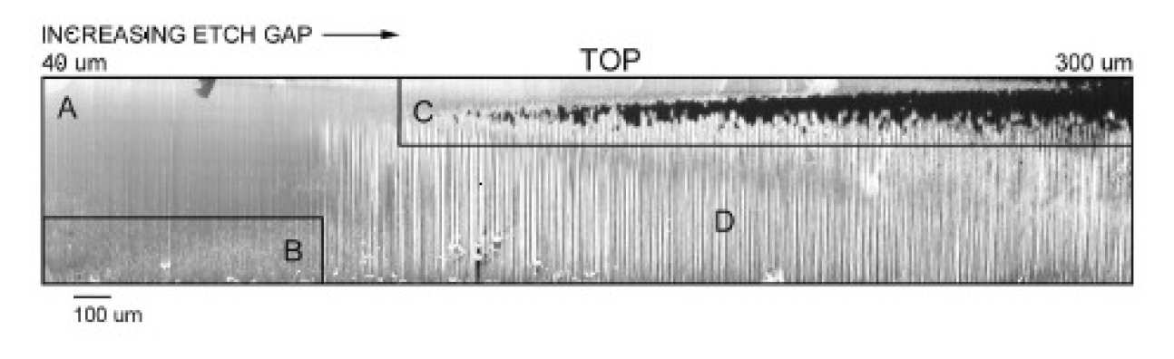
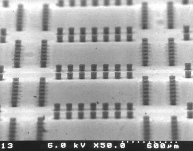
We have analysed the quality of sidewalls resulting from through-wafer deep reactive-ion etching using scanning electron microscopy, atomic-force microscopy and interferometry. Surface quality and profile are very dependent on the width of the etched channel. Channels narrower than 100 µm show generally good sidewall smoothness, though with a bowed profile leading to ion-induced damage towards the bottom of the etch; this appearance is due to overetching of the sidewalls. Thicker channels, in contrast, exhibit overpassivation of the sidewalls with a region of thick polymer buildup followed by vertical striations and very a rough surface but with an overall vertical profile. Onset of surface roughness is associated with increased processing rather than initial mask roughness. Redeposition of the passivation from the trench bottom to the sidewalls is suggested as an explanation of these observations.
 |
|---|
|
Sidewall quality as a function of the width of the etch trench. Area A has good |
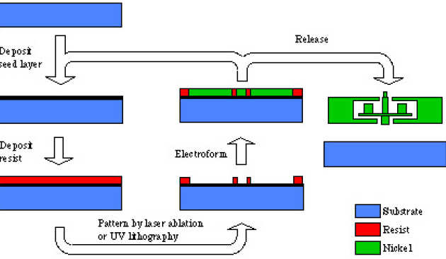
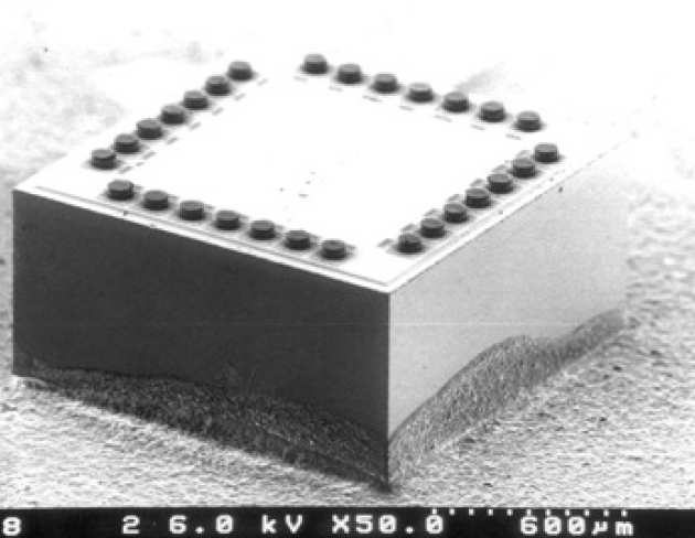
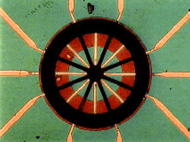
The high cost of the X-ray LIGA process has led to widespread research into alternative methods for realising three-dimensional microstructures. We have developed a low-cost 'Laser-LIGA' process based on electroforming of polymer moulds formed by excimer laser ablation. This process can produce nickel structures with depths of up to several hundred microns and with surface roughnesses down to 100 nm. Current developments include the extension of the technique to allow multi-level processing, the formation of structures with complex surface profiles by means of variable lithography.
 |
|---|
| Six-level nickel microturbine fabricated using a combination of of UV- and Laser-LIGA. |
|
|
|---|
|
Multi-level LIGA process combining excimer laser micromachining and conventional lithography. |
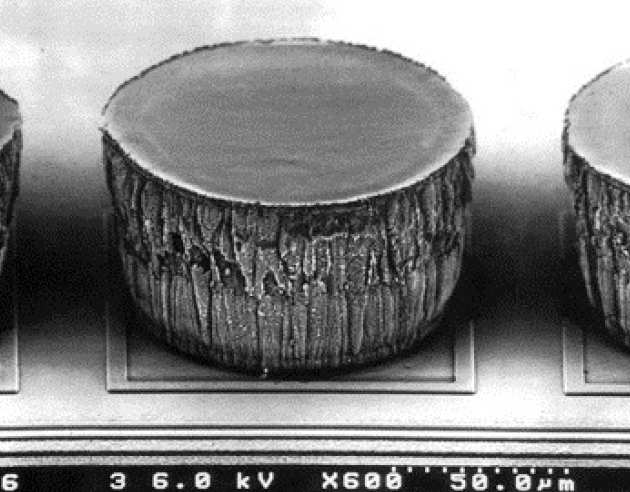
We have developed a novel flip-chip bump bonding technique for silicon microelectronics, in which arrays of metal bumps are first fabricated en masse on a carrier wafer, and then transferred to silicon chips by a laser-driven release process. Copper bumps with gold bonding layers are fabricated on quartz wafers by forming a deep mold by UV lithography and then electroplating bump structures within the mold. The bumps are thermosonically bonded to their respective silicon chips on a die-by-die basis, and then released from the transparent carrier wafer by machining of a sacrificial polyimide layer using pulsed ultra-violet light incident through the carrier from an excimer laser source. The process is inherently parallel, involves minimal processing of the silicon prior to bump attachment, and is scalable to very fine (sub 100 mm) interconnect pitches. It can easily be applied to diced chips. Applications of the process are expected to lie in the packaging of multi-chip modules (MCMs) with high density interconnects.
 | |
|---|---|
|
 |
|---|
| Bump arrays on a quartz carrier. |
 |
|---|
|
Detail of a single bumped contact pad. |
Laser-Assisted Assembly
Microstructures attached to an optically transparent substrate by a polymer sacrificial layer may be released by excimer laser radiation incident through the substrate. We have been investigating a hybrid micro-assembly process based on this principle. The process allows components to be transferred from one wafer to another simply by bringing them into proximity, aligning them, and exposing the upper wafer to a single laser pulse. In addition to allowing direct transfer of parts between wafers in close proximity, laser-driven release offers other advantages over wet chemical release: most importantly, it is rapid, and can be applied selectively by masked exposure.
 |
|---|
| Laser-assembled wobble motor, rotor and stator originally on different substrates. |
| Laser-assisted parallel assembly process |
Andrew Holmes, Carl Paterson (Physics Dept.)
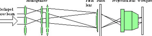
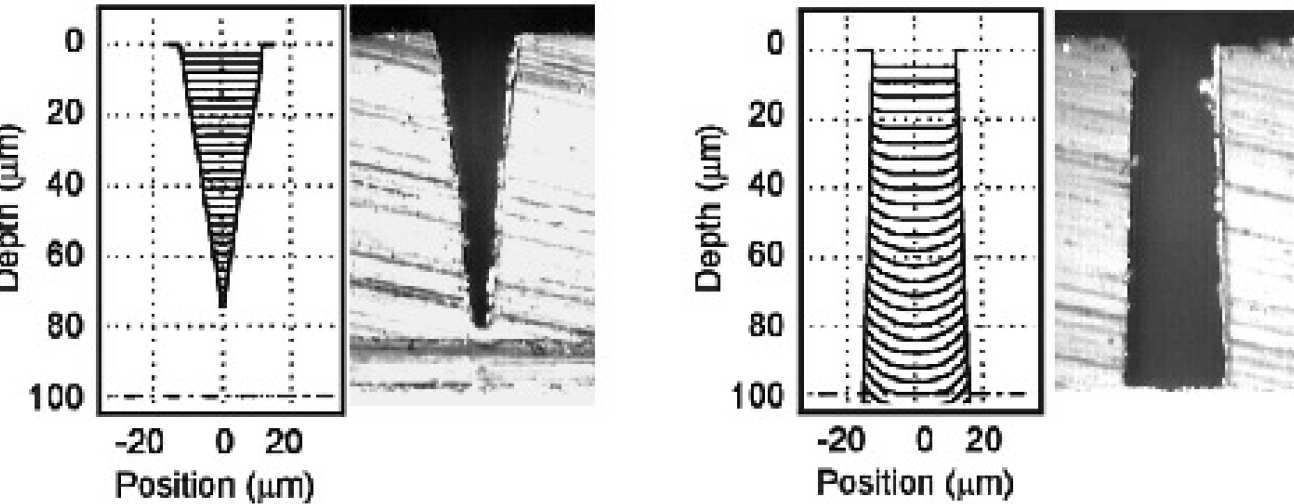
Excimer laser micromachining of polymers, although well established industrially, is still a highly empirical process. In particular, the optimal conditions for each new material or application generally have to be established by experiment. We have been developing a numerical model of the process, with a view to minimising the amount of experimental data required. The model can make quantitative predications about the three-dimensional shaped produced on projection of a given mask pattern, given basic information about the mask, the optical system and the material etch characteristics. By including the illumination system, we have produced the first ablation model that correctly predicts undercut at high numerical apertures and fluences. The figures below show comparisons between the predicted and actual profiles of 25 microns-wide laser machined trenches machined in Du Pont RISTON dry film photoresist, using an Exitech Series 7000 workstation operated at 248 nm wavelength with a 15 x 0.28 NA projection lens. The two trenches were formed with low and high pulse energies, and undercut can clearly be seen in the high energy case.
 |
|---|
| Optical set-up assumed in numerical modelling |
 |
|---|
| Trenches formed with a) 600 pulses at 0.15 Jcm-2 fluence, and b) 600 pulses at 0.5 Jcm-2. The predicted profiles show the evolution of the trench shape at 20-pulse intervals. |
Malcolm Gower and Andrew Holmes
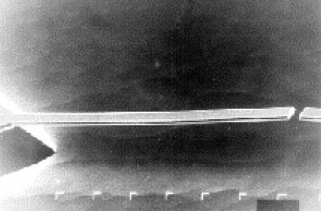
We have developed an optical model for the pulsed laser microablation of materials, a process now in widespread industrial use for drilling microholes - in circuit boards, interconnect packages and ink jet printer nozzles; repairing microelectronic and display devices; scribing solar photovoltaic devices (cells and panels), silicon wafers and ink jet heads; prototyping MEMS devices; manufacturing medical devices and corneal sculpting in corrective refractive eye surgery. This model when applied to femtosecond, picosecond and nanosecond duration laser pulses allows for a complete representation of the laser illumination used as well as the effects the structure can have on modifying the illumination created by previous pulses due to wall reflections and shadowing of the beam by the structure created. The aim of the project is to provide predictions of the shape of the microstructure created solely from a prori knowledge of the laser illumination conditions used.
The example shown pictorially is a pulse-by-pulse sequence of the microablation of a conical hole (shown in yellow) using a 248nm wavelength laser beam focussed into the middle of a plastic block of polyimide.
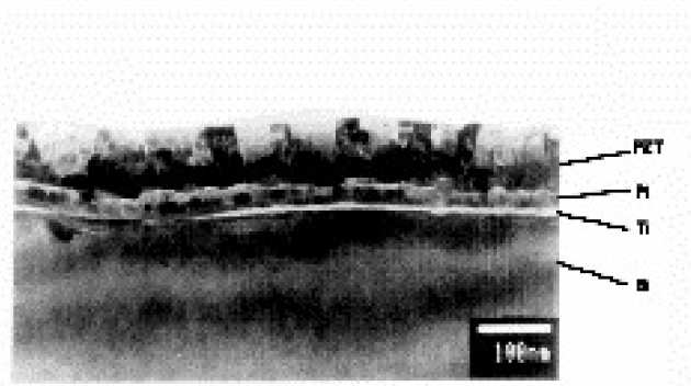
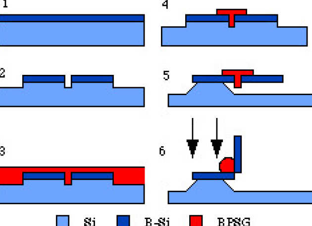
The most practical techniques for micro-actuation are the piezoelectric and electrostatic mechanisms. Of these, piezoelectric materials offer the best possibility of high forces in limited volumes and simple geometries; to date, however, realisation of this potential has been limited by the difficulties in depositing and processing the piezoelectric layers. We have developed a metallo-organic decomposition (MOD) solution route for depositing thin piezoelectric films of Pb(Zr0.53Ti0.47)O3(PZT), based on repeated cycles of spin-coating and annealing. Crystallisation is then carried out by further heat treatment to obtain the desired perovskite phase and orientation. Careful choice of electrode material and process parameters has been necessary to prevent problems of interdiffusion and chemical reactions between substrate and film (shown in the cross-sectional transmission electron micrograph below), to obtain together the required crystalline phase, microstructure, electrical properties (see below) and device fabrication compatibility. We have developed wet- and dry-etching processes for PZT, and have fabricated cantilever beam actuators as shown above. These consist of Si/PZT bilayers, patterned by lithography and reactive ion etching followed by anisotropic etching of the underlying Si.
 |
|---|
| Piezoelectric bimorph actuator based on a silicon cantilever beam with a PZT active layer. |
 |
|---|
| XTEM photograph of PZT film shows interdiffusion in the PZT/Pt/Ti/Si system. Introducing SiO2between Si and Ti solves this problem. |
 |
|---|
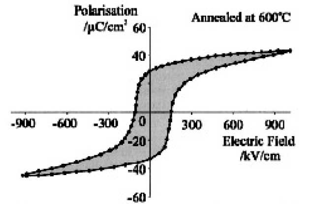
| P-E Loop for PZT film on Pt/Ti/SiO2/Si:Pr = 30 mC/cm2, Ec = 150 kV/cm |
Jiebin Gu, W. T. Pike and W. J. Karl
We have developed a solder-pump technology to create through silicon via (TSV) using the Gibbs-Thomson capillary effect with the liquid formed from molten solder balls [1]. The folded-reservoir structure of the solder-pump (Figure. 1) is formed by mounting a device wafer on top of a printing reservoir structure separated by a spacer. The via holes are surrounded by solder wettable metal pads on both sides of the wafer to produce a solid bond between the solder and the device wafer after reflow. The printing reservoir structure, providing sufficient solder volume to fill the entire via hole after reflow, is formed by a feed and underpass wafer. The spacer between the device wafer and the feed wafer creates a gap to allow the solder to wet the metal pad on the bottom of the wafer. As none of these components is bonded during reflow, the print structure can be repeatedly reused.
The solder-pump technology makes use of a pressure differential created by liquid surface tension to drive molten solder between capillaries of varying diameters. The pressure difference can be derived as
(1)
Where γ is the surface tension of molten solder and r1, r2 are the radii of the through-wafer holes. To ensure that the flow drives the molten solder into the device-wafer via, the geometry requires . The working principle of the reservoir solder-pump is illustrated in Figure 2. Because of the condition that , there is a continuous pressure difference between the head and the end of the molten solder column during reflow, until finally the solder fills the via hole and an equilibrium state is reached. The Reflow results can be found below.
The advantages of the solder pump technology
1.No metallization is needed in the sidewall of the via hole.
2.Once the solder balls melt, it only takes seconds to flow and fill the via hole.
3.No special wafer is needed. This technology is also not limited to silicon substrate. Any material that is unwettable to liquid solder is implementable.
The figure below illustrated a promising via-last way to form TSV based on the solder pump technology.
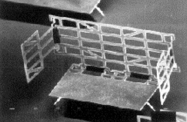
One problem with conventional methods of microstructure fabrication is that they involve two-dimensional pattern transfer, and hence yield only quasi three-dimensional structures. We have proposed that microstructures can be reconfigured into full three-dimensional geometries, using the surface tension force of molten solder or glass to perform out-of-plane rotation of flexible hinges. By considering the equilibrium of a hinged structure with a free liquid boundary, we have shown that the hinge will rotate until the boundary is minimised and that the angle of rotation can be controlled by the volume of liquid. In the microstructure domain, surface tension forces can greatly exceed gravitational forces. As a result, the surface tension torque is sufficient to rotate parts with the dimensions of typical micro-mechanical devices. The method has recently been demonstrated using parts from both Si and electroplated nickel, and assembly of complex three-dimensional microstructures has also been performed based on a simple latching mechanism designed to ensure accurate 90o rotation.
 |
|---|
| Multiple silicon flaps self-assembled into position using the surface tension force of molten glass. |
 |
|---|
| Schematic of operation. |
 |
|---|
|
Detail of latching mechanism. |