Room-Temperature Single Atom Silicon Quantum Electronics
EPSRC Single-Atom Quantum Electrons project (EP/V030035/1)
Background
Single atom quantum dot (QD) transistors, where discrete, quantum confined electronic states combined with single-electron charging allow charge to be controlled at the level of one electron [1-2], reduce electronic devices to their ultimate limit of ~1 nm or even smaller. Operating as atomic-scale single-electron transistors (SETs) [1-2], these devices hold great promise for a wide range of applications, from ultra-low power, highly scaled nanoelectronics, to quantum computation, single charge/molecule detection, and metrology current standards.
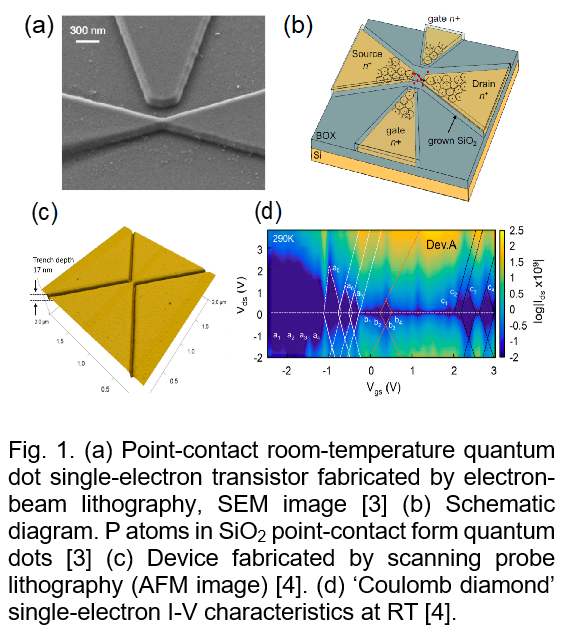
Practical applications of SETs, e.g., nanoelectronics or single-molecule sensing, require both room-temperature (RT) operation and large-scale manufacturability. RT SETs/QDs (Fig. 1) in silicon enable scaling of information bits to their ultimate level of one electron per bit while retaining LSI circuit compatibility. Furthermore, the ultra-high charge sensitivity (<1e) of SETs may allow sensing of single charges or molecules. Finally, unlike ‘classical’ transistors, SET/QD electrical characteristics improve with size downscaling, enabling a transition from ‘classical’ to highly scaled, low power quantum nanoelectronics.
SETs and QDs exploit the single-electron charging energy Ec = e2/2C and quantum confined states Ek of a tunnel-coupled conducting ‘island’ with capacitance C, to control the tunnel current [3]. For RT operation, Ec, Ek and the tunnel barrier must be >> kBT = 26 meV, requiring QDs <10 nm where C ~ 1 aF and Ec and Ek > 0.1 eV. Recently, at Imperial College London (ICL), we have raised single atom SET/QD operation to RT [6-9], using P atom QDs embedded in Si-SiO2-Si point-contact transistors fabricated by electron-beam lithography (EBL) (Fig. 1(a)). P atoms embedded within a SiO2 tunnel barrier formed deep potential wells (~1 eV) suitable for RT operation.
Aims and objectives: Room-temperature single atom electronics
Project aims
This project aims to develop RT single-atom devices, circuits and sensors in Si, compatible with large-scale manufacturing processes. RT single-atom quantum dot transistors (SA-QDTs) using dopant atoms embedded in SiO2 will form the basic circuit element. We propose to build memory, logic and single-particle sensing devices and circuits using EBL and scanning probe lithography (SPL) methods. The project partners include Imperial College London (EBL nanofabrication), University College London (UCL, SPL nanofabrication), and A-Modelling Solutions (Device simulations). The ultra-high resolution SPL techniques use a novel combination of the techniques of scanning tunnelling microscopy (STM) hydrogen lithography and atomic force microscopy (AFM) generated local anodic oxidation to fabricate single atom devices at precise atomic locations. A combination of the ICL and UCL approaches will ultimately be used to achieve and atomically precise, RT QD device technology.
Project objectives
- Simultaneous operation of 3 SA-QDTs, each device operating with 1-5 QDs.
- Apply SA-QDTs to single-molecule sensing.
- Fabricate ‘proof-of-principle’ RT memory and logic circuits.
- Develop all scanning probe, single-atom position-controlled devices.
- Integrate STM fabricated, position-controlled devices (O4) within EBL fabricated point-contact transistor structures.
- Develop simulation methods and tools.
Accordion widget for research list
Imperial College London (ICL)
The Imperial College London Optical and Semiconductor Devices (OSD) group has a long-standing, internationally leading position in the design, nanofabrication, and measurement of single-electron and quantum dot devices [3], particularly devices capable of room-temperature operation [3-6], with a view to practical, nanoelectronics applications. Recently, this work has led to significant breakthroughs, with the first demonstration of room-temperature operation in single-dopant atom quantum dot [4], and double quantum dot [6], transistors in silicon, compatible with conventional silicon nanoelectronics circuit technology. The group has a further interest in establishing single nanometre scale nanolithography and tool development, using both conventional electron-beam and novel atomic force microscope-based scanning probe methods. This includes the first demonstration of silicon quantum dot transistors using scanning probe methods [4].
University College London (UCL)
The UCL group specialises in the fabrication, study and exploitation of buried dopant devices in silicon whose dimensions vary from tens of nanometres to single atoms. A major recent breakthrough was to use a new dopant atom in the fabrication process, with arsenic replacing phosphorus [7], giving world-leading advantages due to the benefits as brings to fabrication and quantum device design [7]. They have also developed different scanning probe techniques to image buried dopant structures, such as 3-D donor designs [8] and nanoscale n-p junctions [9]. This follows from scanning tunnelling microscopy (STM) research, imaging single donor wave functions [10] and buried phosphorus nanostructures [11]. In addition, they have built and measured artificial molecular states from chemical bonds [12] and proposed measuring a topological phase transition in a chain of dopant atoms [13].
A-Modelling Solutions Ltd
Dr Aleksey Andreev, Company Director at A-Modelling Solutions Ltd, is a non-academic partner of the project, responsible for simulations and modelling work. He has interests in multiscale simulations of nanoscale devices, and predictive theory and modelling development for advanced quantum technologies. Recently, this has included work on single atom devices, in collaboration with ICL [7, 9]. He has >25 years of research experience both in academic institutes and in industry. He has been a Senior Research Scientist at Hitachi Cambridge Laboratory and a Senior Lecturer at the University of Surrey. He has also been a private consultant for DERA, later Qiteniq, working on a number of different projects, including a 5+ year project with Intel, leading work on the theory and modelling of novel transistors. He has co-authored more than 100 papers and 12 patents.
- Zahid Durrani et al, 2022, "Room temperature Szilard cycle and entropy exchange at the Landauer limit in a dopant atom double quantum dot silicon transistor" J. Phys. D: Appl. Phys. 55 285304.
- Faris Abualnaja, Wenkun He, Mervyn Jones, Zahid Durrani, 2022, "Device fabrication for investigating Maxwell's Demon at room-temperature using double quantum dot transistors in silicon", Micro and Nano Engineering Vol:14, pp.100114.
- Abualnaja F, He W, Jones M, Durrani Z. 2021. "Room-temperature double quantum dot transistors for investigating Maxwell's Demon." [Poster]. Micro and Nano Engineering, Torino, Italy.
- He W, Chu K, Abualnaja F, Jones M, Durrani Z. 2022."Dark-field optical fault detection for point-contact single electron transistos." Micro and Nano Engineering, Leuven, Belgium.
- Durrani Z. 2022. "Information entropy exchange and the Szilard cycle in a room-temperature dopant atom double quantum dot transistor." 2D Material and Quantum Effect Devices, Islamabad, Pakistan.
References
- K. Likharev, Proceedings of the IEEE 87, 606 (1999).
- Z. A. K. Durrani, Imperial College Press, (2010).
- Z. Durrani et al. Nanotechnology 28, 125208 (2017).
- Z. Durrani et al. J. Appl. Phys. 124, 144502 (2018).
- C. Rawlings et al. Nanotechnology 29, 505302 (2018).
- F. Abualnaja et al, Phys. Rev. Appl. 12, 064050 (2019).
- T. J. Z. Stock et al. ACS Nano 14, 3316 (2020).
- G. Gramse et al. Sci. Adv. 3, e1602586 (2017).
- G. Gramse et al. Nat. Electron. In Press (2020).
- K. Sinthiptharakoon et al. J. Phys.: Cond. Mat. 26, 012001 (2014).
- L. Oberbeck et al. Appl. Phys. Letts. 104, 253102 (2014).
- S. R. Schofield et al. Nat. Comms. 4, 1649 (2013).
- N. H. Le et al. npj Quantum Info. 6, 24 (2020).