Optics
- Electrochromics
- Waveguide Devices by Electron Beam Irradiation of Silica
- Sol-gel Silicate Glasses
- Silica-on-silicon Waveguide Devices Fabricated by SC-RTA
- Erbium doped waveguide amplifiers (EDWAs)
- Wideband Integrated Optical Amplifiers
- Planar Waveguide Optical Amplifiers
- Multi-Valued Modulation Schemes For Optical Communications
- Folded dipole plasmonic resonators
- Cylindrical plasmonic nano-antennas
- Loss and Thermal Noise in Plasmonic Waveguides
Mino Green, James Hampson, Valerie Stevens
The colouration of certain transition metal oxides in their highest oxidation state (eg. WO3, V2O5, etc.) by the reversible formation of their oxide bronze is the basis of several types of electrochromic device. Research into the underlying materials as well as fabrication and testing of electrochromic displays and windows has been carried out in the Group for the past two decades. Topics currently under investigation are:
1. New methods of bronze formation by chemical or electrochemical means.
2. Other bronze forming thin film materials.
3. New electrochromic mirror configurations.
4. Measurement of mean grain size of thin films as a function of preparative conditions, using microscopy, chemical etch rate and x-ray diffraction (the la s t in collaboration with the University of Padova).
5. Automated electrochromic win dow fabrication.
 |
|---|
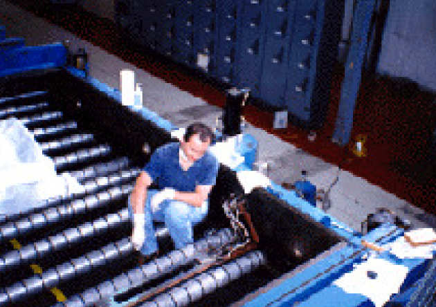
| Installation of a strip-source for vacuum deposition of WO3 in an industrial plant |
 |
|---|
| Prototype modular equipment for electrochromic window fabrication |
Richard Syms, Tom Tate, Ary Syahriar
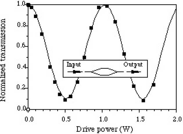
We have developed a method of fabricating channel optical waveguides in thick layers of PECVD silica-on-silicon by electron beam irradiation. An electron-stopping mask is first constructed on the silica surface, by electroplating a thick gold layer around a photoresist pattern. The patterned surface is then irradiated with a high current electron beam of moderate (25 keV) energy. Electrons that penetrate through openings in the mask cause defects in the silica lattice, which give rise to dimensional and refractive index changes. The defects are being studied by electron spin resonance (ESR). The refractive index changes are in the range 4 x 10⁻³ - 8 x 10⁻³, i.e., sufficient for waveguide formation. With careful preprocessing, O-H contamination can be virtually eliminated, yielding spectrally flat, polarization-independent performance, with propagation losses as low as 0.1 dB/cm at IR wavelengths. The method has been used for the construction of a range of devices, including tapers, thermo-optic interferometric modulators, directional couplers and tree-structured power splitters. Bidirectional tuning of directional couplers made by more conventional methods to elimate fabrication tolerances has also been demonstrated.
 |
|---|
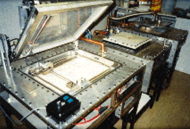
| Electron irradiation plant |
 |
|---|
| Titanium heater electrodes in a thermo-optic interferometric modulator |
 |
|---|
| Power-transmission characteristic of a thermo-optic modulator |
Richard Syms, Eric Yeatman, Mino Green, Huang Weibin
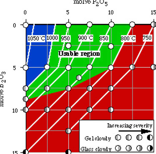
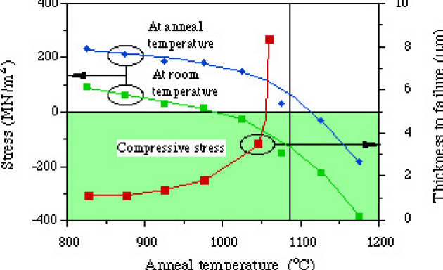
We have developed a method for deposition of thick (> 30 microns) layers of silica and doped silica on silicon substrates, based on the repetitive use of spin-coating and rapid thermal annealing (SC-RTA). Cracking of such thick films is prevented by careful control of the film stress so that the glass is always under tension, even at elevated temperatures. Stable precursor recipes and compositional maps of materials that can be deposited have been obtained for a wide range of different silicate glass systems. These include silica doped with titanium, germanium, boron, phosphorus, aluminium, gallium, neodymium, erbium and ytterbium. Materials such as phosphosilicate glass (PSG) can be deposited without the use of the extremely hazardous chemicals such as phosphine needed in equivalent CVD and PECVD processes.
 |
|---|
| Locus of usable compositions in the sol-gel BPSG system |
 |
|---|
| Variation of film stress and number of layers before cracking with annealing temperature, for sol-gel silica-titania |
Richard Syms, Vitor Schneider, Huang Weibin
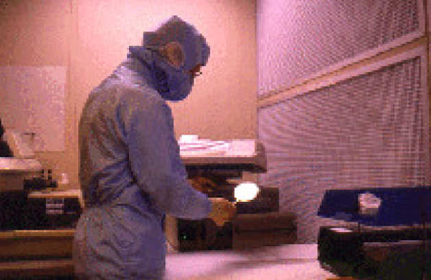
We have developed a method for deposition of thick (> 30 microns) layers of silica and doped silica on silicon substrates, based on the repetitive use of spin-coating and rapid thermal annealing (SC-RTA). Cracking of such thick films is prevented by careful control of the film stress so that the glass is always under tension, even at elevated temperatures. The glass layers are used in the fabrication of silica-on-silicon planar lightwave circuits, following the conventional route of reactive ion etching to form topographic waveguide cores, followed by reflow and burial. Strip loaded waveguides have also been demonstrated. Channel guides have been demonstrated in a variety of materials systems, including silica-titania, phosphosilicate glass (PSG), borophosphosilicate glass (BPSG) and germanophosphosilicate glass (GPSG). Spectrally flat, polarization-independent propagation losses as low as 0.2 dB/cm have been obtained at near infrared wavelengths (1.5 microns) using GPSG. Passive components such as Y-junction tree-structured power splitters have been demonstrated, together with thermo-optic interferometric modulators driven by titanium surface heater electrodes. Fibre-pigtailed devices have also been constructed, based on anisotropic etching of the silicon substrate to provide V-groove alignment features for ribbon fibre pigtails. Gallium doping is now being investigated, with a view to obtaining an improved passive host for active dopants such as erbium.
 |
|---|
| The SC-RTA process being performed |
 |
|---|
| Packaged silica-on silicon device |
 |
|---|
| Bends and branches in sol-gel waveguides before cladding |
Eric Yeatman, Richard Syms, Munir Ahmad, Huang Weibin, Athanasios Laliotis
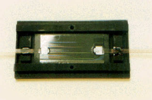
The introduc tion of erbium-doped fibre amplifiers (EDFAs) has greatly benefited the implementation of fibre optic l inks operating at 1.5 µm waveleng th, by reducing the need for electronic regeneration of very high bandwidth signals. Even greater benefits could be realised from ampli fiers in planar form, where they could be integrated with other functions. This could compensate for insertion losses in passive components, particularly those key components (e.g. star couplers and wavelength demultiplexers) which need to split the incoming power among a number of outputs.
The main challenge in developing a planar glass waveguide amplifier lies in achieving the required gain over a short path, which requires very high dopant levels. We are investigating the insertion of Er and other rare-earth dopants in sol-gel silica-on-silicon waveguides, to form erbium doped waveguide amplifiers (EDWAs). The sol gel glass is deposited by repetitive cycles of spin coating and rapid thermal annealing. Because of the great flexibility of the process, a relatively large number of glass constituents may easily be combined together,
By minimising the process temperatures, and choosing the co-dopants carefully, we have now demonstrated Er-doped channel guides with an internal gain of 1.35 dB/cm, the highest figure demonstrated for erbium doped silica-on-silicon to date. Low fibre coupling loss has also been obtained, so that net fibre-device-fibre gain can be achieved.
 |
|---|
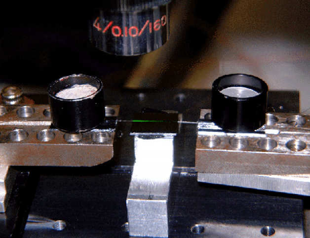
| Erbium-doped channel waveguide silica-on-silicon optical amplifier formed in sol-gel glass. The green streak arises from upconversion |
 |
|---|
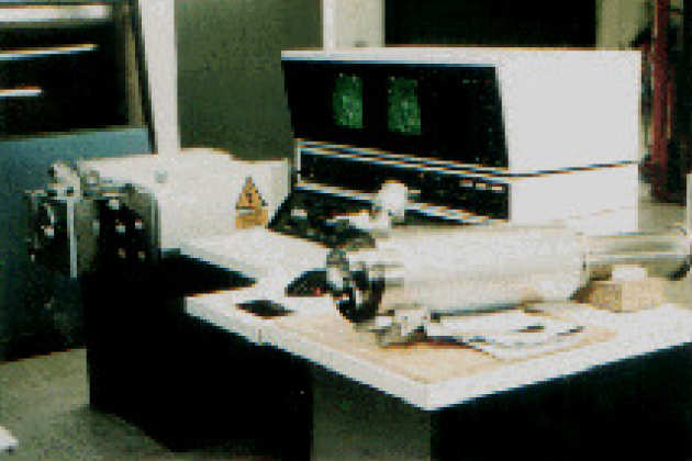
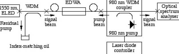
| Arrangement for measurement of erbium doped waveguide amplifiers |
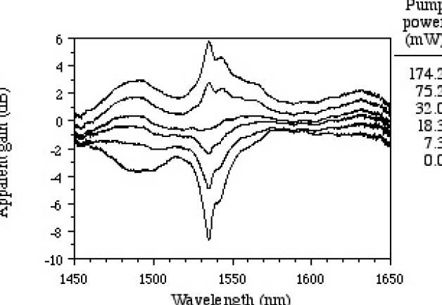 |
|---|
| Transmission spectra obtained from 5.5 cm long EDWA, showing almost complete inversion at high pump powers |
Eric Yeatman, Athanasios Laliotis
Silica on silicon is a popular format for integrated optic devices, having excellent compatibility with optical fibre, high integration potential and low cost. However, devices to date have mainly been passive, because of the limited functional capabilities of silica glass. Previously, a method of fabricating glass waveguides on silicon using the sol-gel system was developed in this group, and erbium doping was used to demonstrate waveguide amplifiers. However, the gain bandwidth achieved was low, because of the limited amounts and combinations of co-dopants that could be employed.
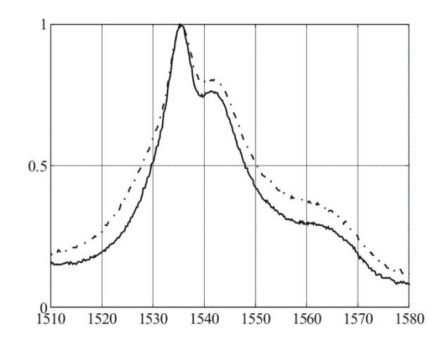
In this project, we take advantage of the multiple layer coating process of sol-gel glasses to achieve spectral properties not possible in a uniform glass. The approach is to deposit the core of the waveguide using alternate layers having different co-dopant compositions, and thus gain spectra, such that the final waveguide has the optical properties of a uniform core, but with spectral properties which are a composite of the individual layers. By this method, the potential for gain of 1.4 dB/cm is shown, over a 20 nm spectral range.
 |
|---|
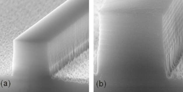
| SEM pictures of laminated amplifier. (a) Waveguide cross section prior to cladding deposition. (b) After an HF etching step to enhance the contrast between individual layers, which are clearly visible |
 |
|---|
| Normalized emission cross sections of laminated amplifier (dashed-dotted line) and alumino-phosphosilicate (solid line) amplifier (TH3) |
Richard Syms, Huang Weibin
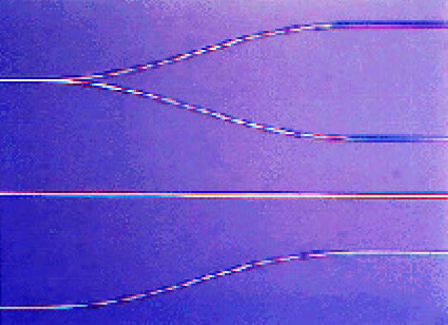
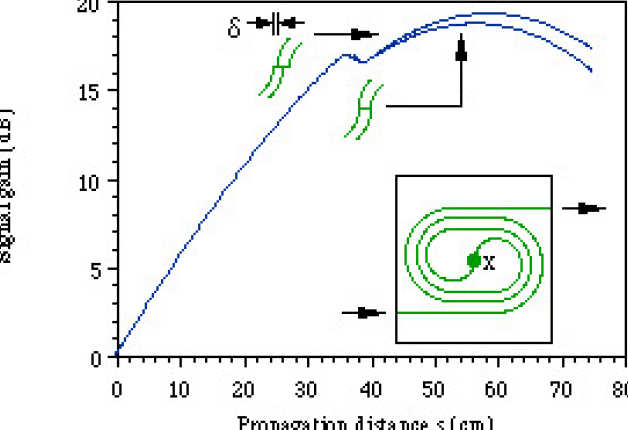
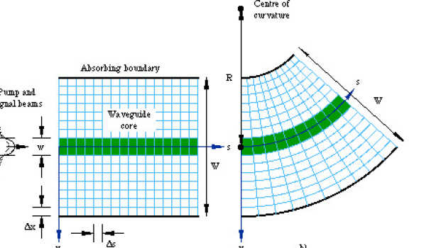
Layouts containing curved guides with small bend radii will be needed to minimise the size of planar erbium doped planar waveguide amplifiers (EDWAs). Curved waveguides cannot guide electromagnetic fields without radiation loss. Furthermore, the transverse fields of both the pump and the signal beam are distorted in bend sections, so that the spatial overlap between the two fields and the erbium doped region is lowered. Both these effects make the normal models inaccurate for folded amplifiers. We have developed a numerical model for spiral and folded EDWAs, based on a rate equation model of the local complex dielectric constant and beam propagation by the method of lines. A five-level system is used to describe the ion-ion interactions that occur at high erbium concentrations. Using this model, amplification in both straight and curved slab guides can be simulated.
 |
|---|
| Simulation of folded amplifier layout |
 |
|---|
| Discretion of space in the method of lines model |
Nicholas Avlonitis and Eric Yeatman
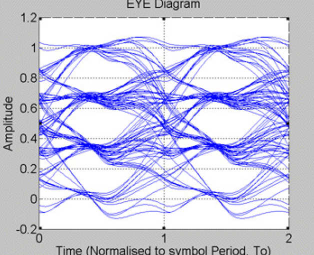
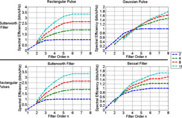
Current optical systems mainly utilise simple on-off keying modulation. The overall spectral efficiency of such systems, used in conjunction with WDM, is limited to below 1 bit/s/Hz. With bit-rate requirements continuously increasing, this limitation is beginning to impinge on system capacity. The aim of this work is to examine the potential of improving the spectral efficiency of optical systems using multi-valued modulation schemes. Initially we have considered primarily the limitations caused by inter-symbol and adjacent channel interference, and the influence of the amplitude and phase response of the channel separation filter. Results show that substantial spectral efficiency gains become possible using higher order filters, and that the required filter order increases with the number of symbol values. The effects of pulse format (NRZ, RZ) and filter type (Butterworth, Bessel..) have also been determined. We are currently examining the performance of multi-level modulation in the presence of fibre dispersion and nonlinearity.
This project is sponsored by EPSRC and Nortel Networks, and is part of a major UK collaboration, the Ultrafast Photonics Consortium (UPC).
 |
|---|
| Eye diagram for 4-level amplitude shift keying |
 |
|---|
| Spectral efficiency for multi-level ASK as a function of demultiplexing filter order. Large increases in capacity are shown to be possible with higher order filters |
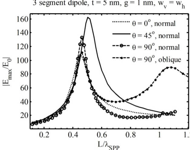
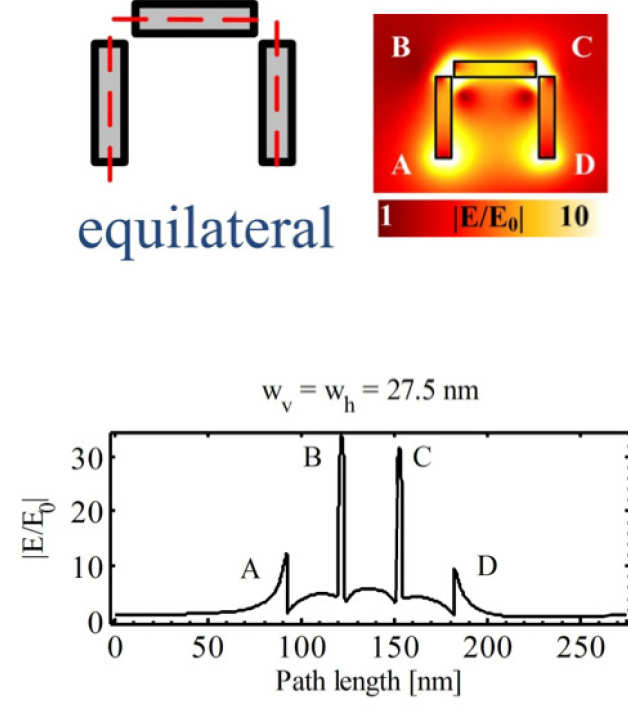
Kaushal Choonee and Richard Syms
We have proposed a new class of folded ordered plasmonic dipole nanoresonators based on insulator-metal-insulator (IMI) slab waveguides. This work is motivated by the development of a novel fabrication process that avoids the need for direct write nanolithography and instead relies on accessible UV lithography and other top-down parallel fabrication techniques that result in metallic dolmen structures with nanometre sized gaps. The dolmen geometry consists of two vertical segments supporting a flat horizontal slab. We have shown using frequency domain finite element analysis that such structures, which are essentially folded dipole antennas, resonate in a similar manner to their linear unfolded counterparts. The effect of the likely fabrication features has also been studied.
 |
|---|
| Geometry of a folded dipole resonator. |
 |
|---|
| Electric field enhancement factor obtained with different fold angles. |
 |
|---|
| 3D and unfolded 2D variations of electric field at resonance. |
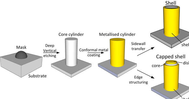
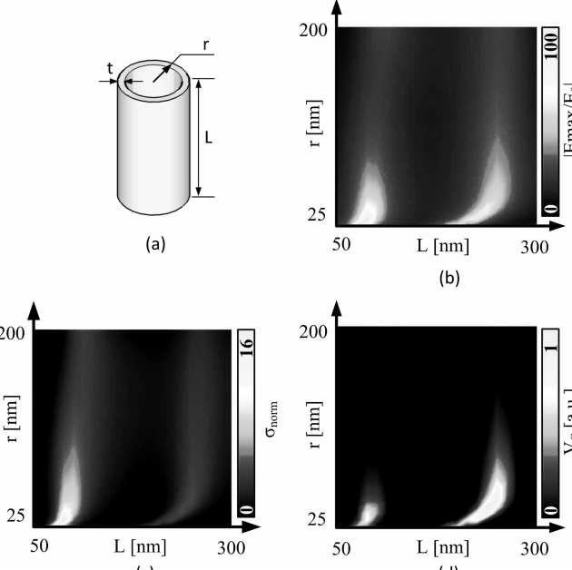
Kaushal Chooneeand Richard Syms
We have proposed a cylindrical metallic plasmonic nano-antenna consisting of a shell supporting a disk, which we term a capped shell. Using frequency domain finite element analysis we have shown that this new topology is weakly dependent on the radius of the structure and is therefore suitable for fabrication by parallel processes such as island lithography, which generates a pseudo-random array of pillars with a distribution of diameters. Furthermore, compared to similar resonators such as rods, disks and shells, the capped shell generates a larger volume with high fields, and is hence useful as a nano-antenna for light-matter interaction.
 |
|---|
| Fabrication for generating the cylindrical structures. The starting point is a mask defined by island lithography, which determines the radius of the nano-resonator. |
 |
|---|
| a) Shell geometry; b)-d) contour maps showing resonant behaviour as a function of r and L in terms of b) |Emax/E0|, c) σnorm, and d) VC. |
Richard Syms and Laszlo Solymar
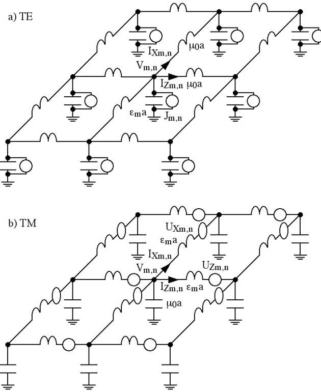
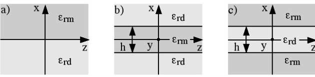
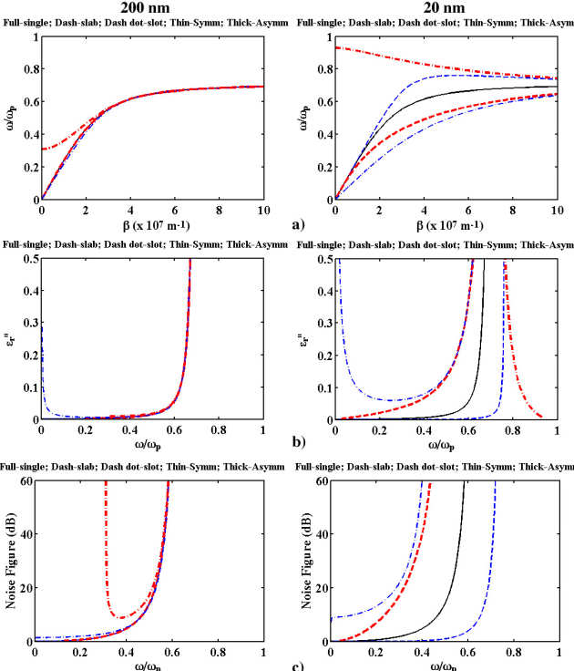
We have used Rytov's theory of thermally generated radiation to find the noise in two-dimensional passive guides based on an arbitrary distribution of lossy isotropic dielectric. To simplify calculations, the Maxwell curl equations are approximated using difference equations that also permit a transmission-line analogy and material losses are assumed to be low enough for modal losses to be estimated using perturbation theory. We have shown that an effective medium representation of each mode is valid for both loss and noise, and hence that a one-dimensional model can be used to estimate the noise factor when a given mode is used in a communications link. This model only requires knowledge of the real and imaginary parts of the modal dielectric constant. The former can be found by solving the lossless eigenvalue problem, while the latter can be estimated using perturbation theory. Because of their high loss, the theory is most relevant to plasmonic waveguides, and its application is demonstrated using single interface, slab and slot guide examples. The best noise performance is offered by the long-range plasmon supported by the slab guide.
 |
|---|
| 2D transmission line models for a) TE and b) TM, with noise sources. |
 |
|---|
| Geometries for a) single-interface, b) slab and c) slot plasmonic waveguides. |
 |
|---|
| a) Dispersion characteristic and b) and c) frequency variation of eru'' and the noise figure for plasmons on single interfaces, slabs and slots. Two sets of data are shown: h = 200 nm (LH) and h = 20 nm (RH). The propagation distance is 10 um. |